Investigations of optical and thermal properties of surface layers of Cd1-xBexTe samples by the photoacoustic method
- Faculty of Electronics and Computer Studies, Technical University of Koszalin, ul. Śniadeckich 2, Koszalin, Poland
- Institute of Physics, Nicolaus Copernicus University, ul. Grudziądzka 5/7, 87-100 Torun, Poland
Article Info
Received 08 Dec. 2023
Received in revised form 22 Mar. 2024
Accepted 15 Apr. 2024
Available on-line 08 May 2024
Keywords: Thermal parameters; optical parameters; surface layers; photoacoustics.
Abstract
The work presents the results of a research on the photoacoustic spectra of thin surface layers of Cd1−xBexTe crystals formed by grinding and polishing their surfaces. As a result of matching the theoretical and experimental photoacoustic spectra, thermal and optical parameters of these layers were determined. Thermal parameters of the surface layers, such as thermal conductivity and thermal diffusivity, turned out to be much worse than the analogous parameters of the substrate. The increase in the optical absorption of surface layers for photon energies below Eg was also determined.
Introduction
AII-BVI mixed semiconductors are interesting as they can be applied in bandgap engineering, i.e., changing the composition of these crystals changes the value of their energy gap. CdTe and CdTe-based mixed crystals, such as Cd1−xBexTe or Cd1−xZnxTe, are promising materials, especially for high efficiency thin film solar cells, X and 𝛾 detectors, and infrared filters.
The surface condition of semiconductor samples has a strong influence on the results of spectroscopic tests and, consequently, on the interpretation of these results. This effect is particularly visible in piezoelectric, photoacoustic, and surface photovoltage spectra. This problem is important because as a result of processing the sample surfaces, several physical parameters of the surface layers change, such as thermal, optical, and recombination parameters. Additionally, a near-surface electric field induced by charged surface levels arises which can also modify the experimental results.
Different measurement methods are applied for investigations of these samples. One group of such methods piezoelectricphotothermal (PZE) method and the other is the photo-acoustic (PA) method, and the photopyroelectric method.
The method of measuring PA spectra with microphonedetection used in the research presented in this work is verysensitive to the optical and thermal parameters of the testedsamples. The basic method used in PA spectroscopy is themethod described in Refs. 1 and 2. However, this methodcan be used for homogeneous single-layer samplesassuming that they are thermally thick. The PA method isalso used to study the optical absorption coefficient spectraof thin films. Application of this method for thin films of Ge and In2S3 deposited on the glass is presented in Refs. 3and 4. Investigations of thin CdTe films also deposited onthe glass are presented in Refs. 5 and 6. Results of PAinvestigations of CuInSn2 thin films are presented inRefs. 7–9. Investigations of CuIn0.75 Ga0.25 Se2 thin filmsare presented in Refs. 10–13 and in 14–16. References 17and 18 present the PA spectral investigations of CuInSe2 thin films. PA spectral investigations of thin film inorganicmaterials are shown in Ref. 19. Investigations of thin filmsof GaInNxAs1−x and CdO+CdTiO3 are presented inRefs. 20–22, respectively. PA investigations of CdSxSe1-xare presented in Ref. 23.
It has been observed that the surface preparationprocess influences the PA PZE spectra as it is presented inRefs. 24 and 25. Application of the PZE method to thestudy of CdTe crystals is described in Ref. 26. In this work, PZE spectra of CdTe crystals wereinterpreted assuming that on the tested sample surface,there is a surface layer with thermal parameters worse thanthose of the substrate. The influence of the surfacecondition on PA spectra is presented in Refs. 27–29.
The influence of the surface treatment of CdZnTe crystals on their recombination and structural parameters ispresented in Refs. 30–33. The influence of the surfacetreatment on the optical absorption coefficient of Si andZnSe crystal samples is presented in Refs. 34, 35, and 36, 37, respectively.
In this work, an attempt has been made to use the PAmethod with microphone detection to study thermal andoptical parameters of the surface layers of Cd1−xBexTe crystals from the theoretical analysis of these PA spectra inthe model of three-layer samples. The paper presents theresults of experimental studies of the PA amplitude andphase spectra of polished and ground Cd1−xBexTe samples.The aim of the research was to determine the thermalparameters of the surface layers, as well as their opticalparameters.
Theoretical model
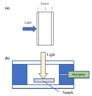
The schematic diagram of the investigated samples ispresented in Fig. 1(a). The samples were described in thethree-layer model in Fig. 1(a). Layers 1 and 3 are thinsurface layers resulting from various surface treatments ofsamples. Layer 2 is an un-defected part of the sample. Eachlayer is described by a set of optical parameters of theoptical absorption spectrum for the energy of photonssmaller than 𝐸g and the energy of photons larger than 𝐸g,and a set of thermal parameters: thermal conductivity,thermal diffusivity, and thickness of these layers.
The samples were placed in a PA chamber. The PAsignal was recorded with a microphone. The experimental configuration applied is called total. A schematic diagram of the PA cell with the sample is presented in Fig. 1(b). In the experiment, the PA amplitude and phase spectra were measured in the photon energy range from 1.2 eV to 1.8 eV. The light modulation frequency was 128 Hz.
Following the theoretical considerations of the temperature for multilayer systems presented in Refs. 38 and 39, the following formula for the total PA signal was derived. The total periodical overpressure in the PA chamber is given by the equation:
\( P_t=\frac{T(0)+T\left(d_t\right)}{\sigma_g} \) (1)
where T(0) and T(dt) are the temperatures of the front (illuminated) and back sides of the sample and are described by the expressions:
\( T(0)=M_1+M_2-E_1 \exp \left(-\beta_1 d_1\right) \) (2)
\( \begin{aligned} T\left(d_t\right)= & M_5 \exp \left(\sigma_3 d_3\right)+M_6 \exp \left(-\sigma_3 d_3\right) \\ & -E_3 \exp \left(-\beta_3 d_3\right) \end{aligned} \) (3)
𝑀1, 𝑀2, 𝑀5, and 𝑀6 are solutions of the set of equations:
\( \begin{aligned} &\text { and }\\ &E_1=\frac{\beta_1}{2 \kappa_1\left(\beta_1-\sigma_1\right)}\\ &\begin{aligned} & M_1-M_2-M_3=E_1 \\ & M_2 \exp \left(\sigma_1 d_1\right)-M_3 \exp \left(-\sigma_1 d_1\right)-M_4-M_5 \\ & =E_1 \exp \left(-\beta_1 d_1\right)-E_2 \\ & M_4 \exp \left(\sigma_2 d_2\right)-M_5 \exp \left(-\sigma_2 d_2\right)-M_6-M_7 \\ & =E_2 \exp \left(-\beta_2 d_2\right)-E_3 \\ & M_6 \exp \left(\sigma_3 d_3\right)-M_7 \exp \left(-\sigma_3 d_3\right)-M_8 \\ & =E_3 \exp \left(-\beta_3 d_3\right) \\ & s_{g 1} M_1-M_2+M_3=\frac{\beta_1}{\sigma_1} E_1 \\ & -M_2 \exp \left(\sigma_1 d_1\right)+M_3 \exp \left(-\sigma_1 d_1\right)+s_{21} M_4-s_{21} M_5 \\ & =\frac{\beta_1}{\sigma_1} E_1 \exp \left(-\beta_1 d_1\right)-\frac{\kappa_2 \beta_2}{\kappa_1 \sigma_1} E_2 \\ & -M_4 \exp \left(\sigma_2 d_2\right)+M_5 \exp \left(-\sigma_2 d_2\right)+s_{32} M_6-s_{32} M_7 \\ & =\frac{\beta_2}{\sigma_2} E_2 \exp \left(-\beta_2 d_2\right)-\frac{\kappa_3 \beta_3}{\kappa_2 \sigma_2} E_3 \\ & -M_6 \exp \left(\sigma_3 d_3\right)-M_7 \exp \left(-\sigma_3 d_3\right)-s_{b 3} M_8 \\ & =\frac{\beta_3}{\sigma_3} E_3 \exp \left(-\beta_3 d_3\right) \end{aligned}\\ &M_1-M_2-M_3=E_1\\ &M_2 \exp \left(\sigma_1 d_1\right)-M_3 \exp \left(-\sigma_1 d_1\right)-M_4-M_5\\ &=E_1 \exp \left(-\beta_1 d_1\right)-E_2\\ &M_4 \exp \left(\sigma_2 d_2\right)-M_5 \exp \left(-\sigma_2 d_2\right)-M_6-M_7\\ &=E_2 \exp \left(-\beta_2 d_2\right)-E_3\\ &M_6 \exp \left(\sigma_3 d_3\right)-M_7 \exp \left(-\sigma_3 d_3\right)-M_8\\ &=E_3 \exp \left(-\beta_3 d_3\right)\\ &s_{g 1} M_1-M_2+M_3=\frac{\beta_1}{\sigma_1} E_1\\ &-M_2 \exp \left(\sigma_1 d_1\right)+M_3 \exp \left(-\sigma_1 d_1\right)+s_{21} M_4-s_{21} M_5\\ &=\frac{\beta_1}{\sigma_1} E_1 \exp \left(-\beta_1 d_1\right)-\frac{\kappa_2 \beta_2}{\kappa_1 \sigma_1} E_2\\ &-M_4 \exp \left(\sigma_2 d_2\right)+M_5 \exp \left(-\sigma_2 d_2\right)+s_{32} M_6-s_{32} M_7\\ &=\frac{\beta_2}{\sigma_2} E_2 \exp \left(-\beta_2 d_2\right)-\frac{\kappa_3 \beta_3}{\kappa_2 \sigma_2} E_3\\ &-M_6 \exp \left(\sigma_3 d_3\right)-M_7 \exp \left(-\sigma_3 d_3\right)-s_{b 3} M_8\\ &=\frac{\beta_3}{\sigma_3} E_3 \exp \left(-\beta_3 d_3\right) \end{aligned} \) (4)
\( E_1=\frac{\beta_1}{2 \kappa_1\left(\beta_1-\sigma_1\right)} \) (5)
\( E_3=\frac{\rho_3}{2 \kappa_3\left(\beta_3-\sigma_3\right)} \exp \left(-\beta_1 d_1-\beta_2 d_2\right) \) (6)
\( \sigma_i=(1+i) \sqrt{\frac{\pi f}{\alpha_i}} \)
where 𝑖 is the index of the layer; indexes 𝑔, 𝑏 mean medium in front and back of the sample (the air in this case); 𝑓 is the frequency; 𝛼 is the thermal diffusivity;
\( s_{i j}=\frac{e_i}{b_j} \)
where 𝑖, 𝑗 indicate the layers: 𝑔, 1, 2, 3, and 𝑏;\( e=\sqrt{\kappa \varrho c_p} \)
is the thermal effusivity; 𝜅 is the thermal conductivity; 𝜌 is the density; 𝑐𝑝 is the specific heat of the material; 𝛽 is the absorption coefficient; 𝑑𝑡 is the total thickness of the sample equal to the sum of thicknesses of the layers 1, 2, and 3.The optical absorption coefficient is described by equation:
\( \begin{cases}\beta_i(E)=\beta_{0 i}+A_{1 i} \cdot \exp \left(\frac{E-E_{\mathrm{g}}}{\gamma \cdot k \cdot T}\right), & \text { for } E \leq E_{\mathrm{g}} \\ \beta_i(E)=A_{0 i}\left(E-E_{\mathrm{g}}\right)^{0.5}, & \text { for } E>E_{\mathrm{g}}\end{cases} \) (6)
where index 𝑖 = 1, 3 denotes the parameters of thesurface layers 1 and 3 and 𝑖=2 denotes the parameters ofthe substrate 2. As a result of matching the theoretical PAamplitude and phase spectra with the experimental PAspectra, the optical and thermal parameters of layers 1 and3 were determined. Thermal parameters of layer 2, i.e.,Cd1−xBexTe substrates were taken from Ref. 40.
They were determined with the photopyroelectricmethod and they are presented in Table 1.
Table 1.
Thermal parameters of the layer 2 Cd1−xBexTe.
Crystal composition x |
Thermal conductivity 𝜿2 (Wm−1K−1) |
Thermal diffusivity 𝜶2 (m2/s) |
0.01 |
4.44 |
3.64e-6 |
0.03 |
2.52 |
2.11e-6 |
0.10 |
2.00 |
1.59e-6 |
Let us assume that the thermal parameters of layers 1 and 3 are equal and denoted with index s. Thicknesses of surface layers: 𝑑𝑠= 2 μm for polished samples and 𝑑𝑠= 6 μm for ground samples. The thickness of layer 2 is 𝑑2= 1 mm.
Sample preparation
Cd1−xBexTe samples were grown from powder using the high-pressure, high-temperature Bridgeman method. The crystal rods were cut into about 1 mm thick samples which were next mechanically surface-treated. The cut samples were ground with the Al2O3 powder, suspended in water, with a grain diameter of 10 μm. Then the samples were polished with diamond paste with grain diameters ranging from 0.1 μm to 1 μm. The samples were next rinsed in water, in ethyl alcohol, and dried.
Experimental results
Experimental PA amplitude and phase of the Cd1−xBexTe and x = 0.01 polished sample are presented in Fig. 2. The description of all symbols and lines used in Fig. 2–Fig. 7 is the following: symbols 1 – diamonds experimental data, line 2 – (blue) PA characteristics for the thermal parameters of thin surface layers the same as those of the bulk and the optical absorption spectra of thin layers are the same as for the bulk and 𝛽02 = 0, line 3 – (green) PA characteristics for the thermal parameters of the surface thin layers the same as those of the bulk (layer 2), but the optical absorption spectra of thin layers are increased by 𝛽0s, line 4 – (red) the best fitting PA characteristics, line 5 – (magenta) PA characteristics for thermal conductivity of thin surface layers 3.16 times smaller and the thermal diffusivity 10 times smaller in comparison to the parameters obtained for the best fitting.

Based on the matching of theoretical PA spectra with experimental ones, the following parameters of surface layers 1 and 3 were determined: 𝜅s = 0.41 Wm−1K−1, 𝛼s = 3 · 10−8 m2/s, 𝛽0s = 337 cm-1, 𝐴1s= 625 cm-1, 𝐸g = 1.49 eV. In the case of PA amplitude spectra [Fig. 2(a)], it can be seen that they mainly change for photon energies below 𝐸g. In this range, the spectra are not very sensitive to the thermal parameters of surface layers but are sensitive to the value of 𝛽0s. However, PA phase spectra are mainly sensitive to thermal parameters [Fig. 2(b)]. The best match between theoretical and experimental characteristics was obtained for curve 4 (red). This match was obtained for the case when the thermal conductivity of thin surface layers was 11 times lower than the thermal conductivity of the substrate (layer 2) and the thermal diffusivity of these layers was as much as 120 times lower than the thermal diffusivity of the substrate. Additionally, a 15-fold increase in the 𝐴1s coefficient was found determining the increase in optical absorption in the Urbach tail area for photon energies below 𝐸g.
Experimental PA amplitude and phase of the Cd1−xBexTe and x = 0.01 ground sample are presented in Fig. 3. Based on matching of theoretical PA spectra with experimental ones, the following parameters were determined: 𝜅s = 0.86 Wm−1K−1, 𝛼s = 20 · 10−8 m2/s, 𝛽0s = 500 cm-1, 𝐴1s= 655 cm-1, Eg = 1.49 eV.

Experimental PA amplitude and phase of the Cd1−xBexTe polished sample and x = 0.03 are presented in Fig. 4. Based on the matching of theoretical PA spectra with experimental ones, the following parameters were determined: 𝜅s = 0.23 Wm−1K−1, 𝛼s = 1.7 · 10−8 m2/s, 𝛽0s = 262 cm-1, 𝐴1s= 719 cm-1, Eg= 1.60 eV.

Experimental PA amplitude and phase of the Cd1−xBexTe ground sample and x = 0.03 are presented in Fig. 5. Based on the matching of theoretical PA spectra with experimental ones, the following parameters were determined: 𝜅s = 1.3 Wm−1K−1, 𝛼s = 42 · 10−8 m2/s, 𝛽0s = 693 cm-1, 𝐴1s= 787 cm-1, Eg = 1.60 eV.

Experimental PA amplitude and phase of the Cd1−xBexTe polished sample and x = 0.1 are presented in Fig. 6. Based on matching of theoretical PA spectra with experimental ones, the following parameters were determined: 𝜅s = 0.15 Wm−1K−1, 𝛼s = 1.0 · 10−8 m2/s, 𝛽0s = 290 cm-1, 𝐴1s= 8.7 · 103 cm-1, Eg= 1.72 eV.

Experimental PA amplitude and phase of the Cd1−xBexTe ground sample and x = 0.1 are presented in Fig. 7.

Based on matching of theoretical PA spectra with experimental ones, the following parameters were determined: 𝜅s = 0.38 Wm−1K−1, 𝛼s = 13 · 10−8 m2/s, 𝛽0s = 391 cm-1, 𝐴1s= 1 · 104 cm-1, Eg = 1.72 eV.
Results
The obtained collected values of thermal and optical parameters of the tested surface layers of investigated samples, resulting from polishing and grinding, are presented in Table 2.
Table 2.
Thermal and optical parameters of surface layers obtained after different
treatments of Cd1−xBexTe samples with different x parameter values.

The average uncertainty in determining the thermal parameters of the surface layers is estimated to be about 10%. The main factor influencing this uncertainty is the estimated value of the thickness of the surface layers. The values of the 𝛽0s parameter were verified using sample transmittance measurements. Examples of transmittance spectra of polished samples for x = 0.01 and x = 0.03 are shown in Fig. 8.

Conclusions
Studies of Cd1−xBexTe mixed crystals for x = 0.01, 0.03, and 0.1, after polishing and grinding, using PA measurement method in the total configuration indicated that it is possible to determine thermal and optical properties of their surface layers.
As a result of theoretical analyses of the amplitude and phase PA spectra, the following parameters of these layers were determined: thermal conductivity 𝜅s, thermal diffusivity 𝛼s, optical absorption coefficient 𝛽0s, and absorption in the Urbach tail 𝐴1s.
It was found out that for polished samples, the thermal conductivity decreased approximately 11 times and the thermal diffusivity decreased approximately 120 times. The optical absorption coefficient 𝛽0s increased from 0 to about 300 cm-1 and the Urbach tail coefficient 𝐴1sincreased on average about 12 times. These parameters illustrate the degree of changes in the properties of the above parameters in the thin polished layer in relation to the substrate. In the case of surface layers formed as a result of grinding, the thermal conductivity decreased by approximately 6 times, and the thermal diffusivity decreased by approximately 20 times. The optical absorption coefficient 𝛽0s increased from 0 to about 500 cm-1 and the Urbach tail coefficient increased on average by about 12 times.
The main conclusion that can be drawn is that it is not possible to match the theoretical characteristics with experimental ones by assuming only the increase of the optical absorption of the surface layers. To get the best match, the decrease of thermal parameters of the surface layers respective to the substrate must be also assumed.
Authors’ statement
Research concept and design, B.W. and I.S.M.S.; collection and/or assembly of data, I.S.M.S.; data analysis and interpretation, B.W. and I.S.M.S.; writing the article, I.S.M.S.; critical revision of the article, R.O.; final approval of article, I.S.M.S., R.O. and B.W.
References
-
Ghosh, A. K., Som, K. K., Chatterjee, S. & Chaudhuri, B. K. Photoacoustic spectroscopic study of energy gap, optical absorption, and thermal diffusivity of polycrystalline ZnSexTe1−x (0 < = x < =) alloys. Phys. Rev. B 51, 4842–4848 (1995). https://doi.org/10.1103/physrevb.51.4842
-
Poulet, P., Chambron, J. & Unterreiner, R. Quantitative photoacoustic spectroscopy applied to thermally thick samples.J. Appl. Phys. 51, 1738–1742 (1980). https://doi.org/10.1063/1.327785
-
Bychto, L. & Maliński, M. Determination of the optical absorption coefficient spectra of thin semiconductor layers from their photoacoustic spectra. Int. J. Thermophys. 39, 103 (2018). https://doi.org/10.1007/s10765-018-2424-x
-
Bychto, L. & Malinski, M. Photoacoustic spectroscopy analysis of thin semiconductor samples. Opto-Electron. Rev. 26, 2017–222 (2018). https://doi.org/10.1016/J.OPELRE.2018.06.005
-
Vigil-Galan, O. et al. A study of the optical absorption in CdTe by photoacoustic spectroscopy. J. Mater. Sci. 42, 7176–7179 (2007). https://doi.org/10.1007/S10853-006-1246-6
-
Indrea, E., Deac, I., Barbu, A. & Filip, X. Characterization of laser deposited CdTe and Hg1−xCdxTe thin films. Appl. Surf. Sci. 106, 70–74 (1996). https://doi.org/10.1016/S0169-4332(96)00395-9
-
Zegadi, A. et al. Photoacoustic spectroscopy of CuInSe2 thin films. Thin Solid Films 226, 248–253 (1993). https://doi.org/10.1016/0040-6090(93)90386-4
-
Reddy, K. T. R., Slifkin, M. A. & Weiss, A. M. Study of the Optical Behavior of p-CuInSe2 Films by Photoacoustic Spectroscopy. in Electro-Optics and Microelectronics Proceedings (eds. Lavi, R. & Azoulay, E.) 137–141 (IOP Publishing Ltd, Bristol, 2000).
-
Ahmed, E. et al. Laser annealing of flash-evaporated CuInSe2 thin films. J. Mater. Eng. Perform. 15, 213–217 (2006). https://doi.org/10.1361/105994906X95904
-
Ahmed, E. et al. Impact of annealing processes on the properties of CuIn0.75Ga0.25Se2 thin films. Sol. Energy Mater. Sol. Cells 36, 227–239 (1995). https://doi.org/10.1016/0927-0248(94)00175-8
-
Ahmed, E. et al. Thermal annealing of flash evaporated Cu(In, Ga)Se2 thin films. J. Mater. Process. Technol. 77, 260–265 (1998). https://doi.org/10.1016/S0924-0136(97)00426-3
-
Ahmed, E. et al. Effects of H+Ion Implantation and Annealing on The Properties of CuIn0.75Ga0.25Se2 Thin Films. J. Mater. Eng. Perform. 16, 119–122 (2007).https://doi.org/10.1007/s11665-006-9019-6
-
Ahmed, E., Zegadi, A., Hill, A. E., Pilkington, R. D. & Tomlinson, R. D. Optical properties of flash-evaporated CuIn0.75Ga0.25Se2 thin films by photoacoustic spectroscopy. Thin Solid Films 268, 144–151 (1995). https://doi.org/10.1016/0040-6090(95)06811-2
-
Reddy, K. R., Chalapathy, R. B., Slifkin, M. A., Weiß, A. W. & Miles, R. W. Photoacoustic spectroscopy of sprayed CuGaxIn1−xSe2 thin films. Thin Solid Films 387, 205–207 (2001). https://doi.org/10.1016/S0040-6090(00)01713-2
-
Ahmed, E. et al. The influence of annealing processes on the structural, compositional and electro-optical properties of CuIn0.75Ga0.25Se2 thin films. J. Mater. Sci.: Mater. Electron. 7, 213–219 (1996). https://doi.org/10.1007/BF00133118
-
Ahmed, E. et al. Transmission photoacoustic spectroscopy of flash- evaporated CuIn0.75Ga0.25Se2 thin films. Thin Solid Films 515, 239–244 (2006). https://doi.org/10.1016/J.TSF.2005.12.076
-
Viktorov, I. A. et al. Investigation of CuInSe2 films by the method of photoacoustic spectroscopy. J. Appl. Spectrosc. 66, 659–663 (1999). https://doi.org/10.1007/BF02675406
-
Ahmed, E. et al. Laser annealing of flash-evaporated CuInSe2 thin films. J. Mater. Eng Perform. 15, 213–217 (2006). https://doi.org/10.1361/105994906X95904
-
Reddy, K. R., Slifkin, M. A. & Weiss, A. M. Characterization of inorganic materials with photoacoustic spectrophotometry. Opt. Mater. 16, 87–91 (2001). https://doi.org/10.1016/S0925-3467(00)00063-X
-
Cardona-Bedoya, J. A., Gordillo-Delgado, F., Zelaya-Angel, O., Cruz-Orea, A. & Mendoza-Alvarez, J. G. Growth and characteri- zation of GaInNxAs1−x thin films with band-gap energies in the red- blue portion of the visible spectrum. Appl. Phys. Lett. 80, 1900–1902 (2002). https://doi.org/10.1063/1.1454209
-
Mayén-Hernández, S. A. et al. CdO+CdTiO3 thin films prepared by sol-gel. Sol. Energy Mater. Sol. Cells 90, 2280–2288 (2006). https://doi.org/10.1016/J.SOLMAT.2006.03.001
-
Mayén-Hernández, S. A., Torres-Delgado, G., Castanedo-Pérez, R., Mendoza-Álvarez, J. G. & Zelaya-Ángel, O. Optical and structural properties of CdO+CdTiO3 thin films prepared by sol–gel. Mater. Chem. Phys. 115, 530–535 (2009). https://doi.org/10.1016/J.MATCHEMPHYS.2008.11.046
-
Shen, Q., Yuichiro Kato, Y. K. & Taro Toyoda, T. T. Photoacoustic and photoluminescence studies of CdSxSe1−x doped glasses. Jpn. J. Appl. Phys. 36, 3297 (1997). https://doi.org/10.1143/JJAP.36.3297
-
Zakrzewski, J. et al. Photothermal investigation of surface defects of pure semiconducting A2B6 materials. Int. J. Thermophys. 33, 733– 740 (2012). https://doi.org/10.1007/s10765-012-1199-8
-
Strzałkowski, K., Kulesza, S., Zakrzewski, J. & Malinski, M. Surface investigations of ZnBeMnSe mixed crystals by means of the piezoelectric spectroscopy and the AFM technique. Appl. Surf. Sci. 290, 27–34 (2014). https://doi.org/10.1016/J.APSUSC.2013.10.180
-
Zakrzewski, J., Strzałkowski, K., Malinski, M. & Chrobak, Ł. Two- layer model in piezoelectric photothermal spectra of CdTe Crystals. Int. J. Thermophys. 40, 1–10 (2019). https://doi.org/10.1007/S10765-019-2521-5
-
Maliński M. & Bychto L. The Influence of The Quality of CdTe Surface on The Photoacoustic Characteristics. in 28th German Annual Conference on Acoustics DAGA 2002 432–433 (German Acoustic Society, 2002). http://pub.dega-akustik.de/DAGA_1999-2008/data/articles/000748.pdf
-
Bychto L. & Maliński M. The Influence of The Quality of Semiconductor Surface on The Photoacoustic Signal Characteristics on The Example of CdTe studies. in 5th International Workshop on Thermal Investigations of ICs and Microstructures (THERMINIC 1999) 231–235 (IEEE, 1999).
-
Malinski, M., Bychto, L., Łȩgowski, S., Szatkowski, J. & Zakrzewski, J. Photoacoustic studies of Zn1−xBexSe mixed crystals: two-layer approach. Microelectron. J. 32, 903–910 (2001). https://doi.org/10.1016/S0026-2692(01)00080-5
-
Aqariden, F. et al. Influence of surface polishing on the structural and electronic properties of CdZnTe surfaces. J. Electron. Mater. 41, 2893–2898 (2012). https://doi.org/10.1007/s11664-012-2126-2
-
Zheng, Q. et al. Influence of surface preparation on CdZnTe nuclear radiation detectors. Appl. Surf. Sci. 257, 8742–8746 (2011). https://doi.org/10.1016/J.APSUSC.2011.05.098
-
Tari, S. et al. Impact of surface treatment on the structural and electronic properties of polished CdZnTe surfaces for radiation detectors. J. Electron. Mater. 42, 3252–3258 (2013). https://doi.org/10.1007/s11664-013-2649-1
-
Hossain, A. et al. Novel approach to surface processing for improving the efficiency of CdZnTe detectors. J. Electron. Mater. 43, 2771–2777 (2014). https://doi.org/10.1007/s11664-013-2698-5
-
Malinski, M. & Chrobak, Ł. Numerical analysis of the photoacoustic spectra of silicon samples with differently treated surfaces. Opt. Commun. 283, 1004–1007 (2010). https://doi.org/10.1016/J.OPTCOM.2009.11.029
-
Maliński, M. & Chrobak, Ł. Numerical analysis of absorption and transmission photoacoustic spectra of silicon samples with differently treated surfaces. Opto-Electron. Rev. 19, 46–50 (2011). https://doi.org/10.2478/s11772-010-0064-1
-
Chrobak, Ł., Malinski, M., Zakrzewski, J. & Strzałkowski, K. The photoacoustic spectroscopic investigations of the surface preparation of ZnSe crystals. Surf. Sci. 603, 3282–3285 (2009). https://doi.org/10.1016/J.SUSC.2009.09.014
-
Chrobak, Ł., Malinski, M., Zakrzewski, J. & Strzałkowski, K. The photoacoustic spectroscopic investigations of the surface preparation of ZnSe crystals with the use of the optimization methods. Appl. Surf. Sci. 256, 2458–2461 (2010). https://doi.org/10.1016/J.APSUSC.2009.10.087
-
Fernelius, N. C. Extension of the Rosencwaig‐Gersho photoacoustic spectroscopy theory to include effects of a sample coating. J. Appl. Phys. 51, 650–654 (1980). https://doi.org/10.1063/1.327320
-
Hu, H., Wang, X. & Xu, X. Generalized theory of the photoacoustic effect in a multilayer material. J. Appl. Phys. 86, 3953–3958 (1999). https://doi.org/10.1063/1.371313
-
Singh, D., Strzałkowski, K., Abouais, A. & Alaoui-Belghiti, A. Study of the thermal properties and lattice disorder effects in CdTe– based crystals: CdBeTe, CdMnTe, and CdZnTe. Crystals 12, 1555 (2022). https://doi.org/10.3390/cryst12111555