Comparison of TJ and ITO GaN VCSELs in terms of their frequency characteristics
- Institute of Physics, Lodz University of Technology, ul. Wólczańska 217/221, 93-005 Lodz, Poland
Article Info
Received 21 Feb. 2024
Received in revised form 05 Apr. 2024
Accepted 27 Apr. 2024
Available on-line 18 Jun. 2024
Keywords: VCSELs; nitride; capacitance phenomena; computer modelling.
Abstract
The work focuses on vertical cavity surface emitting lasers (VCSELs) made of nitride materials that emit a wavelength of 445 nm. Two structures were examined: a laser with a tunnel junction and implantation (TJ VCSEL) and an ITO contact (ITO VCSEL). The analysis delves into capacitance phenomena influencing the modulation speed of these lasers. The results highlight differences in active currents between two structures, i.e., currents which contribute to the modulation of the laser emission. According to the authors’ simulations, the TJ VCSEL is more effective in modulating the number of carriers in the active region than the ITO VCSEL, assuming the same modulation amplitude of driving current.
Introduction
Recently, visible light optical communication systems have gained significant popularity. The search for the most efficient emitters for these systems is ongoing and nitride vertical cavity surface emitting lasers (VCSELs) may emerge as promising candidates. Despite not being commercially available at present, discussions about their future applications, particularly in visible light communi-cation (VLC) [1-3] systems, are already underway.
VLC systems fall under the optical wireless commu-nication (OWC) [4-7]. OWC is distinguished by its high capacity and immunity to electromagnetic interference in contrast to the widely used radio frequency (RF) communication, such as Wi-Fi. Due to these challenges, OWC presents itself as a promising alternative to radio communications [8].
In optical data transmission systems, a crucial para-meter is the modulation speed of the emitted light. The modulation rate can be constrained among other factors by the presence of capacitance and resistance in the device structure. In this study, the authors investigate the impact of design parameters of the laser structure on the capacitance phenomena occurring in VCSELs.
Historically, most nitride VCSELs have used an indium tin oxide (ITO) contact due to its high electrical conductivity. The necessity for this layer arises from the inadequate conductivity of the p-type GaN layer. Given that the ITO layer also exhibits high absorption, its positioning in the resonator must be optimized to minimize losses. Instead of ITO structures, tunnel junction (TJ) structures can be created. This allows for a reduction in p-type GaN materials and the use of n-type contacts on both sides of the laser which possess superior electrical properties. TJ can be coupled with implantation to direct the current to the centre of the laser. Both implantation and TJ introduce additional capacitances to the structure. Consequently, this work analyses two types of structures: one with an ITO contact (ITO VCSEL) and another with a TJ (TJ VCSEL).
Computer models
The calculations were conducted using computer models developed by the Photonics Group at Lodz University of Technology, Poland. The models include two separated computer models. The first is a self-consistent thermal-electrical computer model which is based on the finite element method (FEM) [9-11]. The model consists of inter-connected modules for thermal, electrical, gain, and optical calculations. The second model is a capacitance model, facilitating dynamic analysis of the current in a laser biased with a modulated voltage. In these calculations, the authors take into account the evolution of the afore-mentioned model. The validity of this model has been experimentally confirmed [12].
Capacitance model
The capacitance model used in this research is a development of the electrical model used in the static simulations. It is also based on the FEM and uses the same rectangular elements as the static calculations which are performed beforehand. To calculate the AC flow in the structure, the authors describe each element by its complex electrical conductivity in both directions necessary to be considered in cylindrical symmetry. The real part of the conductivity is the same as in the static model (where only real values are considered), while the imaginary part is given by the following formula:
\( \operatorname{Im}(\sigma)=i \varepsilon \varepsilon_0 \omega \) (1)
where 𝜀 0 is the vacuum permittivity, 𝜀 is the relative permittivity of the considered element, and 𝜔 is the angular frequency of the alternating component of the bias voltage.
Formally, calculations in the static and AC calculations are very similar. The difference is that the calculations are performed in the complex domain. However, there is a significant difference in the practical implementation of the algorithm and different numerical methods are used in the static and the AC stage of the electrical calculations.
The results provided by the AC calculations are the distributions of the alternating component of the current density distribution given in the standard phasor formalism. This allows for calculation of the impedance of the entire device, but also allows for investigating the capacitance phenomena in different areas of the laser. The parts of the device which are responsible for its capacitance can be identified by analysing distribution of the electric field energy density. The elements where that energy is high give a high contribution to the device capacitance.
In this model, the authors define a parameter which can be useful to verify to what extend capacitance phenomena degrade the laser performance. Generally, with increasing modulation frequency, the modulation current amplitude increases (the modulus of the impedance decreases). This, however, does not necessarily mean that the optical power modulation increase – usually the opposite is true. In order to quantify the useful (from the point of view of optical power modulation) part of the total current, the authors define the active current in the following way:
\( t_{\text {act }}=\left|\int_A \operatorname{Re}(\sigma) \widetilde{U}\right|=\left|\int j_A\right| \) (2)
where 𝐴 denotes the active region aperture, while 𝜎 and 𝑈 are the distribution of the electrical conductivity and the local voltage (both complex) in the aperture, in the AC electrical model. A detailed discussion on the notion of active current can be found in Ref. 13.
Modelled structures
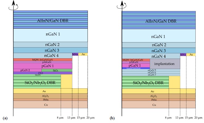
The modelled structures with ITO (ITO VCSELs) are based on a design developed at the Meijo University, Japan, and R&D Laboratories, Stanley Electric Co., Japan [14]. The original structure featured a 10 λ resonator and a 4 μm electrical aperture, designed for an emission wavelength of 445 nm. This structure incorporates hybrid distributed Bragg reflectors (DBRs) with the top DBR made of native materials (46 AlInN/GaN pairs) and the bottom DBR made of dielectrics (10.5 SiO2/Nb2O5pairs). Two types of structures are considered. The first structure closely resembles the original design [Fig. 1(a)]. In this case, the layer limiting the current flow, defining the electrical aperture of the device, is a thin SiO2 layer. The second structure is a modification of the first design. In this VCSEL, a TJ was implemented [Fig. 1(b)]. In the TJ VCSEL design, the electrical aperture of the device in the horizontal direction is defined by the implantation of Al+ ions. This structure is akin to the construction developed at the University of California in Santa Barbara (UCSB), USA [15], with the UCSB structure using two pairs of dielectric DBRs.
Table 1 displays the dimensions of individual VCSEL layers and values of electrical and thermal conductivities.
Table 1.
Properties of layers used in the modelled structures. Thermal and electrical parameters refer to a temperature of 300 K.
Material |
Doping [m−3] |
Thickness [nm] |
Thermal cond. [W/(m ∙K)] |
Electrical cond. [S/m] |
46 pairs AlInN/GaN |
|
4337.8 |
4.87/80.5 |
10/256 |
nGaN 1 |
Si, 1022 |
994.5 |
112 |
126 |
nGaN 2 |
Si, 2.3 · 1024 |
30 |
111 |
8.7 · 103 |
nGaN 3 |
Si, 1025 |
30 |
107 |
2.7 · 104 |
nGaN 4 |
Si, 2.3 · 1024 |
558.1 |
111 |
8.7 · 103 |
MQW |
|
29 |
5 |
|
(InGaN/GaN) pAl0.2GaN |
|
20 |
230 |
19.4 |
ITO VCSEL |
||||
pGaN 1 |
Mg, 1025 |
64.3 |
78 |
71.3 |
pGaN 2 |
Mg, 2 · 1025 |
20 |
75 |
102 |
SiO2 aperture |
|
20 |
1.38 |
0 |
ITO |
|
20 |
3.2 |
105 |
Nb2O5 |
|
35.5 |
1 |
0 |
TJ VCSEL |
||||
pGaN 1 |
|
86 |
27 |
71 |
TJ (p++GaN) |
|
20 |
24 |
5 |
nGaN 5 |
Si, 1.1 · 1026 |
10 |
50 |
1.8 · 105 |
nGaN 6 |
Si, 2.5 · 1024 |
81 |
78 |
3.3 · 104 |
nGaN 7 |
Si, 1.1 · 1026 |
37 |
50 |
1.8 · 105 |
Implantation |
|
116 |
80 |
10−5 |
10.5 pairs SiO2/Nb2O5 |
|
1275.9 |
1.38/1 |
0/0 |
Au |
6 · 103 |
317 |
4.4 · 107 |
|
Al2O3 |
105 |
30 |
1 |
|
PbSn |
5 · 103 |
50 |
1 |
|
Results
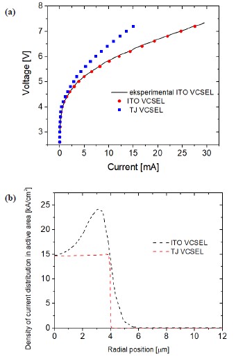
Fig. 2(a) illustrates the static current-voltage characteristics of TJ VCSEL and ITO VCSEL. This figure indicates that the TJ VCSEL exhibits higher resistance compared to the ITO VCSEL structure. In Fig. 2(b), the current density distributions injected into the active area of ITO VCSEL and TJ VCSEL are shown. The TJ structure displays a more uniform current density distribution. The rectangular shape of the TJ VCSEL current distribution is attributed to the method of implementing the structure in such a way that the implantation passes through the active area, as shown in Fig. 1(b).
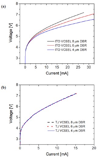
In the subsequent phase, a study was conducted to assess how altering the DBR mirror affects the static characteristics of the lasers. Changes in the mirror width can influence the electrical and thermal properties of the laser and the capacitance calculations to be performed in the next step. Fig. 3 illustrates current-voltage character-istics for both the ITO VCSEL and the TJ VCSEL with lasers having different radii for the bottom DBRs. In the case of ITO VCSELs, structures with smaller radii for the lower DBR exhibit lower resistance. Conversely, in the case of the TJ VCSEL, varying the width of the bottom mirror has minimal effect on the characteristics. This observation is likely associated with the thickness and good conductivity of the n-GaN layer situated between the lower DBR and the implantation. The resistance of the ITO layer in the horizontal direction is high due to the very small thickness of this layer, so when one shortens the path through which the current must flow from the contact to the aperture, one noticeably reduces the laser resistance.
The next stage of the analysis involves a dynamic assessment of lasers. Fig. 4 and 5 present electric field energy density maps for ITO VCSEL and TJ VCSEL, respectively. The areas with high energy of the electric field are the areas which contribute to the device capacitance. Areas highlighted in red (and secondly as yellow) signify laser elements with a high density of the electric field energy. In the case of the ITO VCSEL, these elements encompass the active area and SiO2 aperture. Conversely, for the TJ VCSEL, these areas include the active area and implantation.
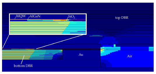
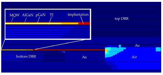
Table 2 presents the energy (𝐸) in both structures for a 1 GHz modulation frequency. These results confirm the information depicted in the energy maps in Fig. 4 and 5, indicating that the highest amount of energy is contained in the MQW, SiO2, and implanted regions.
Table 2.
Density of electric field energy in ITO VCSEL and TJ VCSEL for a 1 GHz modulation frequency for lasers with 8 μm bottom DBRs.
Material |
ITO VCSEL E [fJ] |
ITO VCSEL E [%] |
TJ VCSEL E [fJ] |
TJ VCSEL E [%] |
SiO2 |
2300 |
54.4 |
0.735 |
0.02 |
MQW |
1240 |
29.2 |
477 |
15 |
Air |
575 |
13.6 |
81.7 |
2.56 |
Au-contact |
78.6 |
1.86 |
21.2 |
0.66 |
SiNx |
10.5 |
0.25 |
1.57 |
0.05 |
GaN-DBR |
10.2 |
0.24 |
4.92 |
0.15 |
Nb2O5 |
6.38 |
0.15 |
0.11 |
0.00 |
AlInN |
6.37 |
0.15 |
1.15 |
0.04 |
AlGaN |
3.35 |
0.08 |
5.20 |
0.16 |
GaN |
1.07 |
0.03 |
0.373 |
0.01 |
GaN:Mg_1.00E+25 |
0.811 |
0.02 |
– |
– |
GaN:Mg_2.00E+25 |
0.247 |
0.01 |
– |
– |
Al2O3 |
0.0561 |
0.00 |
0.340 |
0.01 |
ITO |
0.0474 |
0.00 |
– |
– |
Implantation |
– |
– |
2080 |
65.3 |
TJ |
– |
– |
5110 |
16.0 |
pGaN |
– |
– |
1.69 |
0.05 |
Figure 6 illustrates the dependence of the total current flowing through the lasers and the active current as a function of the modulation frequency. Fig. 6(a) and 6(b) indicate that the TJ VCSEL is insensitive to changes in the bottom DBR radius. Conversely, in the ITO VCSEL, the active current increases as the bottom DBR gets narrowed. This phenomenon is attributed to the resistance that ITO introduces to the current flow from the contact to the aperture.
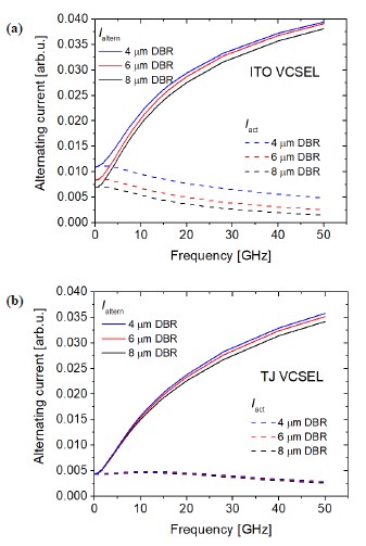
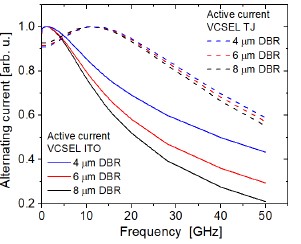
For a more detailed examination of capacitance effects, let us concentrate on active currents. Fig. 7 illustrates the normalised active currents for two types of the VCSELs analysed. A high value of active current indicates better conditions for modulation. Therefore, based on Fig. 7, it can be inferred that for low modulation frequencies (up to approximately 7 GHz), ITO VCSELs perform better in terms of modulation speed. However, for higher frequencies (10–20 GHz), TJ VCSELs exhibit superior performance.
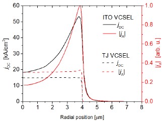
Another thing worth considering is distribution of the active current density, i.e., the integral in (2). The electrical modulation is most effective if it happens at the places where the optical field is the strongest. Considering electrical properties only, the authors cannot make such a comparison, however, they can compare the distribution of the active current with the distribution of the DC component which sustains the laser action. Fig. 8 shows the density of the DC component and the absolute value of the active current density for both constructions considered in this paper. The active current density is presented in arbitrary units because its actual value depends on the amplitude of the voltage modulation, which can be varied in experiment. In both cases, distributions of the static and modulated components are similar, which is generally good. In the ITO VCSEL, the active current shows even stronger current crowding than the DC component which suggests that higher order modes would be modulated more strongly than the fundamental mode.
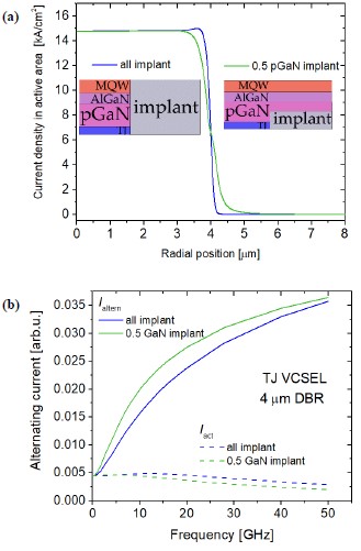
The subsequent step was to investigate how the depth of Al implantation affects the TJ VCSEL modulation speed. Fig. 9 presents the graphs for two considered cases. The first case involves a situation where the laser is implanted to the full depth of the active area, while the second case implants up to half the thickness of the pGaN material. Fig. 9(a) displays the current density distribu-tions and Fig. 9(b) shows the currents de-pending on the modulation frequency. The results indicate that in the latter case, when the laser is implanted to half the GaN thickness, the active current values are slightly worse, indicating that the lasers modulate less efficiently. This is attributed to the fact that thicker implantation results in a smaller capacitance which has a beneficial effect on the modulating properties.
Conclusions
The paper investigates two types of VCSELs: ITO VCSEL and TJ VCSEL. It is observed that TJ VCSELs may offer advantages in terms of modulation speed at higher frequencies compared to ITO VCSELs.
Furthermore, in the case of ITO VCSEL, lasers with a narrower bottom DBR exhibit slightly higher active currents than those with a wider DBR. However, in the case of the TJ VCSEL laser, this difference is negligible.
The thickness of the implanted layer influences the active current. Thinner implantation leads to a deterioration in the ratio between the active and total current. This adverse effect is noticeable even for implantation thick-nesses around 100 nm (although not very strong in this case) and becomes more significant with further reduction in thickness.
Acknowledgements
The work is supported by the project NCN no. UMO-2018/29/N/ST7/02151.
References
-
Strinati, E. C. et al. 6G: The next frontier: From holographic messaging to artificial intelligence using sub-terahertz and visible light communication. IEEE Veh. Technol. Mag. 14, 42–50 (2019). https://doi.org/10.1109/MVT.2019.2921162
-
Céspedes, M. M., Guzmán, B. G. & Jiménez, V. P. Lights and shadows: A comprehensive survey on cooperative and precoding schemes to overcome LOS blockage and interference in indoor VLC. Sensors 21, 861 (2021). https://doi.org/10.3390/s21030861
-
Assabir, A., Elmhamdi, J. & Hammouch, A. Throughput enhance- ment of the edge user equipments based on the powerbandwidth tradeoff in the optical attocell networks. Int. J. Intell. Eng. Syst. 13, 337–355 (2020). https://doi.org/10.22266/ijies2020.1031.31
-
Cao, Z. et al. Reconfigurable beam system for non-line-of-sight free- space optical communication. Light Sci. Appl. 8, 69 (2019). https://doi.org/10.1038/s41377-019-0177-3
-
Mohsan, S. A., Mazinani, A., Sadiq, H. B. & Amjad, H. A survey of optical wireless technologies: Practical considerations, impairments, security issues and future research directions. Opt. Quantum Electron. 54, 187 (2022). https://doi.org/10.1007/s11082-021-03442-5
-
Hameed, S. M., Abdulsatar, S. M. & Sabri, A. A. BER comparison and enhancement of different optical OFDM for VLC. Int. J. Intell. Eng. Syst. 14, 326–336 (2021).https://doi.org/10.22266/ijies2021.0831.29
-
Chowdhury, M. Z., Hossan, M. T., Islam, A. & Jang, Y. M. A comparative survey of optical wireless technologies: Architectures and applications. IEEE Access 16, 9819–9840 (2018). https://doi.org/10.1109/ACCESS.2018.2792419
-
Zhang, L. et al. High-speed multi-user optical wireless communi- cation between VCSEL-integrated electronic devices. Opt. Commun. 486, 126774 (2021). https://doi.org/10.1016/j.optcom.2021.126774
-
Piskorski, Ł., Wasiak, M., Sarzała, R. P. & Nakwaski, W. Tuning effects in optimisation of GaAs-based InGaAs/GaAs quantum-dot VCSELs. Opt. Commun. 281, 3163–3170 (2008).https://doi.org/10.1016/j.optcom.2008.02.011
-
Xu, D. et al. Room-temperature continuous-wave operation of the In(Ga)As/GaAs quantum-dot VCSELs for the 1.3 μm optical-fibre communication. Semicond. Sci. Technol. 24, 055003 (2009). https://doi.org/10.1088/0268-1242/24/5/055003
-
Sarzała, R. P. et al. Numerical self-consistent analysis of VCSELs. Adv. Opt. Technol. 2012, 689519 (2012).https://doi.org/10.1155/2012/689519
-
Wasiak, M. et al. Numerical model of capacitance in vertical-cavity surface-emitting lasers. J. Phys. D: Appl. Phys. 49, 175104 (2016). https://doi.org/10.1088/0022-3727/49/17/175104
-
Wasiak, M. & Sarzała, R. P. Numerical model of capacitance-related phenomena in semiconductor lasers based on partial differential equations. Opto-Electron. Rev. 32, e150606 (2024). https://doi.org/10.24425/opelre.2024.150606
-
Kuramoto, M. et al. High-power GaN-based vertical-cavity surface- emitting lasers with AlInN/GaN distributed Bragg reflectors. Appl.Sci. 9, 416 (2019). https://doi.org/10.3390/app9030416
-
Forman, C. A. et al. Continuous-wave operation of m-plane GaN- based vertical-cavity surface-emitting lasers with a tunnel junction intracavity contact. Appl. Phys. Lett. 112, 111106, (2018). https://doi.org/10.1063/1.5007746