Numerical model of capacitance-related phenomena in semiconductor lasers based on partial differential equations
- Institute of Physics, Lodz University of Technology, ul. Wólczańska 217/221, 93-005 Lodz, Poland
Article Info
Received 24 Feb. 2024
Accepted 01 Apr. 2024
Available on-line 28 Jun. 2024
Keywords: capacitance; finite element methods; semi-conductor lasers.
Abstract
This paper presents a model of the capacitance and electrical properties of semiconductor lasers biased with modulated voltage. The model is based on the finite-element method (FEM), which is widely used in computer modelling and is a natural generalisation of a wellknown constant-voltage FEM electrical model. In principle, the model can be applied to any kind of device where inductance can be neglected. Here, it is applied to simulate the complex impedance and other high-frequency electrical properties of a vertical-cavity surface-emitting laser. These properties are very important for the application of such lasers in optical data transfer systems. The results show that both the diameter of the top mesa and the surface area of the top electrical contact have a strong impact on the performance of the laser. This impact is analysed as a function of the modulation frequency.
Introduction
With the demand for ever greater capacity in telecommunication links, optical data transfer systems are becoming increasingly important. Semiconductor lasers are key components in optical data transfer systems. Edge-emitting semiconductor lasers (EELs) have long been used in longdistance transmission systems. Such systems have allowed for the enormous development of the internet. In recent years, short-distance links have also become very important, steadily replacing copper-wire electrical links. In short-range optical systems, vertical-cavity surface-emitting lasers (VCSELs) are usually used as light emitters. These semiconductor lasers have many advantages over EELs in applications where the power emitted by a single laser need not be very high. Because of their convenient vertical emission, low production costs, very small size, and very low power consumption, VCSELs are well-suited for use in short-range links.
The VCSEL structure contains elements that are sources of capacitance. Besides the p-i-n junction, which is the active region of the VCSEL, there are also insulating layers that direct current towards the centre of the laser. In optical links, where lasers are driven by modulated currents with very high frequencies, capacitance can adversely impact the optical response of the laser to modulation. To measure the electrical properties of a laser at different frequencies, a small-signal modulation (SSM) reflection experiment is commonly used. This experiment allows the complex impedance ˜𝑍 of the tested device to be determined as a function of the modulation frequency 𝑓 . Despite being in optical links, the lasers are modulated with large-amplitude, in general non-sinusoidal, signals. SSM reflection and response provide important information on the expected large-signal performance and are a primary modulation characterisation technique not limited to lasers or light emitters in general [1–4].
To calculate ˜𝑍 ( 𝑓 ) curves, previous studies have used a model based on equivalent circuits containing multiple resistors and capacitors [5–8]. This approach has certain advantages, including the fact that the circuit can be easily integrated with other circuits to describe, for instance, a laser driver. The values for resistance and capacitance are often fitted to the results of SSM experiments. In Ref. [8], a method was presented for numerical determination of the values of elements in a VCSEL circuit. This method allows for analysis of frequency-dependent electrical properties for a given laser design, rather than analysing experimental characteristics.
One, possibly severe, drawback of the circuit-based model is the fact that the circuits generally neglect the lateral direction of the current flow. This approach may therefore fail to take into account important phenomena related to lateral current transport in VCSELs. Moreover, it gives no information regarding the lateral distribution of either the intensity or the phase of carrier injection into the active region. It is a well-known and intuitive fact that in the case of CW laser operation the current distribution has a decisive impact on which of all the possible cavity modes do in fact lase. Similarly, the distribution of the alternating-current (AC) component determines which of the lasing modes will be modulated with the highest amplitude. If the distribution of the direct-current (DC) component were significantly different from that of DC component, then it is possible that the strongest mode would not be modulated most strongly. If the phase of theAC component changed significantly with the lateral position in the active region, then different parts of the active region would be modulated at different moments within the period of modulation. Therefore, it would be very useful to be able to determine the lateral distribution of the complex density of the AC component.
In principle, appropriate elements could be included in the equivalent circuits, although this would increase the number of parameters that have to be fitted to the experiment. However, with increasing numbers of fitting parameters the results tend to become less reliable. The method of least squares finds a local minimum of the sum of squared residuals; but, except in the simplest cases, there can be many such minima. The minimum is determined by the starting values of the parameters, so very different sets of parameters can be found depending on the initial guess. In situations where two or more parameters have a similar impact on the computed value, this method may fail to find the parameters. As a result, circuits that are fitted to experiments cannot in practice be expanded significantly. Moreover, in circuit-based numerical models, the choice of the few elements in the circuit is to some extent arbitrary and the elements are not strictly related to specific areas in the laser volume. To avoid this problem, the finite-element method (FEM) can be used to numerically model the static parameters of the laser.
In our simulations, we first performstatic simulations and then, using some of the results from there, perform AC simulations. This approach is equivalent to finding solutions for a huge lumped circuit, in which each finite element would be represented by two resistors and two capacitors. In the continuity limit, the circuit is transformed into awell-known differential operator. The distributions of different parameters describing the AC component of the driving electric current can be found in the vertical and lateral dimensions, something that was not possible in the simple circuit approach. In the next section, this new FEM-based model is presented in detail along with further results of simulations showing the important insights the model can provide.
Model
The model is applied to the current flow in a VCSEL biased with voltage with a DC or an AC component. First, the capacitance- and inductance-related phenomena in an AC-biased device is analysed. Then, theDCmodel is briefly described. Finally, it is shown how the two models can be connected.
AC phenomena
The standard definition of capacitance uses the notion of electric charge. However, the notion of an electromagnetic field is much more general, and can be used instead [9]. The capacitance of any volume between two equipotential surfaces can then be expressed as
\( C=\frac{2 \mathcal{E}}{U^2} \) (1)
where E is the energy of the electric field in the considered volume and 𝑈 is the potential difference. As an example, consider a uniform material of electric conductivity 𝜎 and relative permittivity 𝜀, through which a uniform current density 𝒋 is flowing. If one selects a cuboid with its base facets perpendicular to 𝒋, then the voltage 𝑈 between them is equal to ∥𝑬∥𝑑, where 𝑑 is the height of the cuboid (the distance between the bases) and 𝑬 = 𝒋/𝜎 is the electric field. The energy of the electric field in the cuboid is then E = 𝜀𝑆𝑑∥ 𝒋 ∥2/(2𝜎2) = 𝜀𝜀0𝑆𝑈2/(2𝑑). The resulting capacitance is described by the well-known parallel-plate capacitor formula: 𝐶 = 𝜀𝜀0𝑆/𝑑. As a result, the cuboid can be represented in an equivalent circuit as a resistor and capacitor connected in parallel. For a sinusoidal current of angular frequency 𝜔, the admittance of this element would be
\( \tilde{Y}=\left(\sigma+i \omega \varepsilon \varepsilon_0\right) \frac{S}{d}=\tilde{\sigma} \frac{S}{d} \) (2)
Consequently, for sinusoidal AC electric potentials the following standard equation can be used:
\( \tilde{j}=-\tilde{\sigma} \nabla \tilde{V} \) (3)
where ˜𝑉 and ˜𝒋 are the complex-valued electric potential and current density in the standard phasor formalism, respectively. The symbol ˜ is used to denote that the value is complex. As a result, the electric potential distribution ˜ 𝑉 in a homogeneous (which in this case means that the material parameters are continuous functions of position) conducting medium can be described by the following partial differential equation (PDE):
\( \nabla(\tilde{\sigma}(\boldsymbol{r}) \nabla \tilde{V}(\boldsymbol{r}))=0 \) (4)
where 𝒓 = (𝑥, 𝑦, 𝑧). On the borders where the material changes (the parameters are discontinuous), the border conditions are given by the condition of continuity of the potential and current density. Equation (4) is applied for all materials in the laser, including the junction. In general, the junction is a non-linear element, but the assumption that the amplitude of the modulation is small means that the junction can be approximated as a linear element whose differential conductivity Re( ˜𝜎) is determined by the DC component of the driving current. The appropriate considerations are presented at the end of the next section.
In the model, there are no electric charges that appear explicitly. However, the charge distribution is determined by the distribution of the electric field.
Equations (4) and (3) describe the electric current in a linear medium under an alternating sinusoidal bias if the inductance-related phenomena can be neglected. In general they cannot, because the skin effect changes the current distribution (compared to the DC case) and increases the resistance. The self inductance affects the imaginary part of the total impedance. The skin depth can be calculated using the following formula [10]:
\( \delta=\sqrt{\frac{2}{\sigma \omega \mu \mu_0}} \) (5)
where 𝜇 is the permeability of the medium. In a GaAsbased semiconductor laser, it can be assumed that the conductivity of the p-type materials is not higher than 104 S/m. The n-type materials may have conductivities of between 5 · 104 S/m and 105 S/m. The modulation frequencies that have been measured in experiments have so far usually been below 50 GHz (a limit also imposed by the measuring equipment). All the materials used to fabricate a semiconductor laser are generally non-magnetic, so 𝜇 = 1. With these values, the following estimates are obtained for skin depth in the p-doped and n-doped parts of the laser diode, respectively:
\( \delta_{\mathrm{p}}>20 \mu \mathrm{m} \quad \delta_{\mathrm{n}}>7 \mu \mathrm{m} \) (6)
In a typical VCSEL, the dimensions of the conducting materials in the laser p-side are significantly smaller than 𝛿p, so the skin effect can be neglected as long as the frequencies are not significantly higher than 50 GHz. On the n-side, however, the situation is not so simple. VCSELs may have n-type electrodes either on the bottom surface of the substrate or in the form of a ring located slightly below the junction, usually near the level of the first distributed Bragg reflector (DBR) layers counting from the bottom (as presented in Section 3, Fig. 1). The configuration in which the n-type electrodes are on the bottom surface of the substrate is not used in VCSELs designed for fast modulation. In a configuration in which both electrodes are located on the top surface of the laser chip, the current flows generally horizontally from the electric aperture at the centre of the active region to the ring contact just below the top surface. In this configuration, the skin effect does not change the current path. Because of the very high conductivity of n-type AlGaAs alloys, the resistance increase related to the skin effect is negligible.
Another effect that should be considered is the inductance of the laser. Because the current flowbetween the electrodes in the top-electrode configuration is mainly horizontal. The inductance of the laser can be estimated using the formula for the inductance of a coaxial conductor with an inner radius equal to that of the aperture 𝑟a and an outer radius equal to the n-type ring contact inner radius 𝑟nc. The distance from the top electrode to the aperture is much smaller, so it can be neglected in this rough estimate. Estimating 𝑟a > 1 μm and 𝑟nc < 100 μm and the effective vertical cross-section of the horizontal current flow as < 10 μm, one obtains the following estimate for laser inductance:
\( L<10 \mathrm{pH} . \) (7)
At 50 GHz, the reactance related to an inductance of 10 pH is equal to 𝜋 Ω, so it is negligible compared to the impedance of the whole device (see Section 3 for actual numbers). These considerations show that, in the case of the lasers analysed in this paper, the impact of inductance can be neglected. However, there are many other cases of lasers in which a model of inductance would be useful.
DC case
Equations describing the electric field, charge distribution, and similar electrical parameters are generally nonlinear and very complicated to solve. Devices such as VCSELs have many junctions. As well as the active-region p-i-n junction, there are interfaces between different materials (metal electrodes are deposited on a semiconductor material, different semiconductor materials are in contact). However, since the resulting junction effect would require a much higher voltage to make current flow through the device, the structures are designed in such a way that junction effects can be avoided. In particular, the DBRs in VCSELs consist of tens of pairs of materials with different refractive indices. In GaAs-based VCSELs, which are by far the most commonly fabricated VCSELs, the DBRs are usually electrically-conductive and made from pairs of AlGaAs layers with different Al compositions. To avoid unwanted junction effects, the high- and low-Al-composition layers are separated by thin layers with graded compositions. These graded layers deteriorate the optical properties, but are necessary for the current to flow through the DBRs. In the case of metal-semiconductor contacts, the semiconductor layer is doped and intermediate metal layers are placed between the semiconductor and the electrode to obtain Ohmic characteristics. In a standard, properly fabricated semiconductor laser, the only nonlinear element is the p-i-n junction. From the point of view of modeling the electrical properties of such devices under a DC bias, this means that simple linear PDEs (with real-valued 𝜎 and 𝑉) can be used (except in the active region).
\( \nabla(\sigma(\boldsymbol{r}) \nabla V(r))=0 \) (8)
Although (8) does not provide a proper description of the microscopic electric field distribution in the semiconductor structure, it can be considered as an equation for the potential which is added to the complicated potential distribution present in the device for an external bias equal to 0. This equation has the same form as (4), except that all the functions and parameters are real-valued.
The static electric properties of semiconductor lasers can be correctly modelled using the linear PDE (8) for the whole device except the p-i-n junction. For the junction, a diode equation is used in the following form:
\( j(x, y)=j_s \exp (\beta U(x, y)) \) (9)
where 𝑗 is the perpendicular (to the junction) component of the current density, 𝑈 is the local voltage on the junction. Using this equation, one can determine conductivity of the junction, which depends on the local voltage:
\( \sigma_{\mathrm{j}}{ }^{(0)}=h \frac{j}{U}=h \frac{j_s \exp (\beta U(x, y))}{U} \) (10)
where ℎ is the thickness of the active region. The values of 𝜎j (0) (𝑥, 𝑦) are determined in a self-consistent loop in the electrical model of the laser.
In the AC model, in (4), ˜𝜎 denotes the complex differential conductivity. The distinction between differential and ordinary conductivity is important only in the non-linear active region. Using (9), one obtains:
\( h \frac{d j}{d U}=\sigma_{\mathrm{j}}^{\text {diff }}=h \beta j=\beta U \sigma_{\mathrm{j}}^{(0)}=\sigma_{\mathrm{j}}{ }^{(0)} \log \frac{j}{j_s} \) (11)
This value can be expressed in a different manner:
\( \sigma_{\mathrm{j}}^{\text {diff }}=\beta U \sigma_{\mathrm{j}}^{(0)}=\sigma_{\mathrm{j}}^{(0)} \log \frac{j}{j_s} \) (12)
The above differential conductivity is the real part of the junction conductivity used in the AC model, so it can be expressed using (2), the complex conductivity of the junction, as:
\( \tilde{\sigma}_j=\sigma_j^{\text {diff }}+i \omega \varepsilon \varepsilon_0 \) (13)
Application to semiconductor lasers
To analyse the performance of a semiconductor laser in real situations, it is necessary to simulate the electrical properties of a laser biased with a voltage𝑈, which has a constant component 𝑈DC and a small modulated component 𝑈AC:
\( U(t)=U_{\mathrm{DC}}+U_{\mathrm{AC}} \cos (\omega t) \) (14)
The amplitude 𝑈AC must be small enough so that the nonlinear electrical phenomena occurring in the laser can be neglected.
The calculations are performed in two steps. First, selfconsistent electrical and thermal simulations of the constant bias 𝑈DC are performed. This step is the same as in the model described in Section 2.2. The calculations are performed using software developed by the authors and described in Ref. [8]. The temperature and potential distributions found at this stage are used to determine the parameters that will be used in the subsequent AC simulations. Most importantly, we determine electrical differential conductivity in the highly nonlinear junction. This depends on the local current density (or voltage), so it depends on the lateral position in the junction. The electrical conductivity of the junction is assumed to be uniform in the perpendicular (vertical) direction.
In our model based on an equivalent circuit, the potential distribution obtained in the static simulations is used to construct the circuit and calculate its resistance and capacitance values [8]. The lateral non-uniformity of the laser is not explicitly represented in the circuit (this non-uniformity was taken into account in the values of the circuit elements), and the junction is represented by a single resistor and capacitor. Although this works well for global parameters such as the laser impedance, in this initial approximation it is not possible to analyse the lateral distribution of the current density. Additionally, the choice of the number of elements in the circuit is to a certain extent arbitrary, although in Ref. [11] we previously showed that the results provided by the model are very similar for circuits with different numbers of elements.
In the second step of the calculations, full simulations of capacitance-related phenomena were performed by solving (4) for selected modulation frequencies, and complex material conductivities using (2) based on the results of the DC simulations performed in the first step. The values used for dielectric constants are those for the static field, because the proper frequency-dependent values seem to be unavailable in the literature. In general, the dielectric constant of the active region depends on the carrier concentration. According to the analysis presented in Ref. [12], the expected reduction in Re(𝜀) for concentrations in the order of 1018 cm-3 is probably within the uncertainty of the values it was possible to use. It is worth noticing that in a lasing device the carrier concentration depends very weakly on the driving current, so the lack of a relation between 𝜀 and carrier concentration in the active region should not change the results qualitatively. The boundary conditions are two potentials on the laser electrodes, the difference between which is equal to 𝑈AC. In the implementation of the model, FEM was used to solve (4). Since this equation is linear (as a consequence of the assumption that the amplitude of the modulation is small), FEM reduces the problem to finding the solution of a system of linear equations. The matrices used in the first step (for constant voltage) are real. In the second step, the matrix is complex, so with the same dimensions the calculations require at least twice as much memory. Moreover, different algorithms may be needed to solve the linear equations in each step.
The modelled VCSEL has, like most VCSELs, approximately cylindrical symmetry. Therefore, it was possible to perform the numerical computations in 2D. In the implementation of the model, FEM was used with rectangular, 4-node elements. The rectangular elements matched the layer-like structure of the VCSEL and the FEM stiffness matrix was a band matrix, which greatly reduced memory consumption. The mesh used in the calculations contained around 2.2 · 105 elements. The same mesh was used in both the DC (for both thermal and electrical problems) and AC calculations. For the DC model, in which the stiffness matrix is real, we used a LAPACK function, namely dpbsv, to solve the systems of equations for the thermal and electrical problems. The whole self-consistent DC procedure required around 1GB of RAM and took around 11 min to converge. For the AC problem, where the stiffness matrix is complex, we used our own implementation of the conjugate gradient method (which is an iterative method), because the system was too large for the LAPACK zpbsv and for the amount of RAM available. Calculations for a single frequency took around 1.3 h and required 100MB RAM. If a non-iterative method for the complex system were used, the time of the AC computations could probably be shortened to minutes. All the calculations were performed on a PC with a 3.6 GHz processor.
The model of differential capacitance and related phenomena can be considered as valid for situations where a constant above-threshold current is modulated with a small amplitude AC voltage. Therefore, the model can be used to simulate the results of an SSM reflection experiment in which the impedance of the laser is measured. The simulated impedance is calculated using the following formula:
\( \tilde{Z}=\frac{\tilde{U}}{\tilde{I}} \) (15)
where ˜𝑈 is directly defined by the boundary conditions for the AC differential equation (4) and ˜ 𝐼 is the AC current found by calculating the flux of the density ˜𝒋. Impedance, however, does not provide enough information to assess laser performance as a source of modulated radiation. The impedance decreases with rising frequency, because the capacitance increases the admittance of the device. This means that, with the same amplitude of voltage modulation, the amplitude of the modulated current will be higher. What matters, however, is the amplitude of the number of carriers injected and recombining in the active region. Impedance does not provide this information, so an appropriate parameter needs to be defined.
It can be assumed that in the junction the current density has only the vertical component. The (complex) amplitude of the alternating current density is simply a product of the complex conductivity and the gradient of the (complex) potential:
\( \tilde{j}_{\mathrm{j}}(x, y)=-\tilde{\sigma}_{\mathrm{j}}(x, y) \frac{\partial \tilde{V}_{\mathrm{j}}}{\partial z} \) (16)
Since the junction is considered uniform in the vertical direction, this value does not depend on the 𝑧 coordinate if 𝑧 is within the junction. In the phasor formalism, complex current does not necessarily describe the amount of carriers flowing through the element. The part of the total current which does refer to the actual carrier transferred through an element is its projection onto the phasor of the voltage on the element. Consequently, the density of the current which modulates the carrier density in the junction, can be calculated as
\( \tilde{j}_{\mathrm{j}}^{(a)}(x, y)=-\operatorname{Re}\left(\tilde{\sigma}_{\mathrm{j}}(x, y)\right) \frac{\partial \tilde{V}_{\mathrm{j}}}{\partial z} \) (17)
The complex number ˜𝑗j represents the amplitude and the phase shift of the density of carriers injected at 𝑥, 𝑦 into the junction. The phase shift is relative to a certain phase, defined by the phase of the boundary-condition voltage. If the phase of ˜𝑗 (𝑎)j(𝑥, 𝑦) is constant, the number of carriers in the active region is modulated most effectively. In order to calculate the total amplitude of the current that injects carriers into the junction, the following value should be calculated:
\( I_{\mathrm{act}}=\left|\int_{\mathrm{J}} \tilde{J}_{\mathrm{j}}^{(a)}(x, y) d x d y\right| \) (18)
where J denotes the junction plane. We call 𝐼act the active current, because it is responsible for the modulation of the number of photons emitted from the laser junction. The exact relation between the amplitude of the modulation of the injected carriers and the amplitude of the number of photons depends on many factors, including the distributions of both the optical mode(s) and the current density, and is beyond the scope of this work. The active current gives an approximated description on how the effectiveness of the carrier injection changes with the modulation frequency. At the limit of the modulation frequency approaching 0, the active current is equal to the modulus of the total current | ˜ 𝐼 |. Otherwise, it cannot be calculated from the laser impedance.
It is worth noting that although generally |𝐼act | ≤ | ˜ 𝐼 |, it may happen that the active current is greater than the total current. It is possible when the phase of the active-region voltage is not constant along the lateral position and the susceptance of the active region is low relative to the conductance. This is possible when the modulation frequency is low (but higher than 0).
The implementation of this model employs numerical models developed by our group [13]. These numerical models use FEM to solve the PDEs that describe the physical phenomena. Since the model presented above is based on solving standard PDEs, the main formal novelty is the use of complex-valued functions and parameters. It can therefore be implemented using any software capable of such calculations.
Simulations
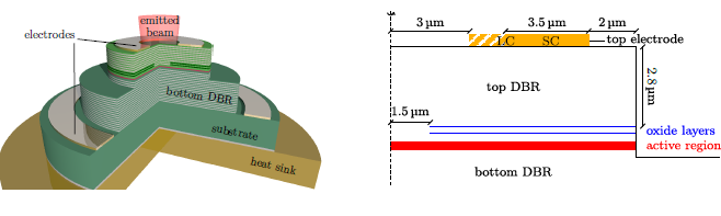
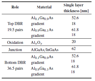
Simulations were performed of the electrical modulation properties of a series of GaAs-based VCSELs. The simulated structures were based on the most typical arsenide VCSELs reported in the literature. The simulated active region consists of five InGaAs quantum wells (QWs). The cavity is confined by two AlGaAs/GaAs DBRs. The top, p-type electrical contact is placed on the top DBR. The bottom, n-type contact surrounds the bottom mesa (Fig. 1). The simulated structures differ in terms of the diameter of the top mesa (from 17 μm to 32 μm), but all have the same electric aperture of 3 μm. The aperture is confined by two 20-nm thick oxide layers located in the first two (counting from the active region) pairs of the p-type DBR. When the mesa diameter is increased, so is the surface of the oxidised layer. The top DBR contains 19.5 pairs. The top contact has the form of a ring, the outer radius of which is 2 μm smaller than the mesa radius. We consider two types of structures, with large (LC) and small (SC) top contacts. In the SC structures, the inner radius of the contact is 3.5 μm smaller than the outer radius (meaning that the width of the top ring contact is 3.5 μm). Structures denoted as LC have an inner radius of 3 μm (1.5 μm from the aperture). For the smallest mesa considered (17 μm in diameter), the LC and SC structures are identical. In all other cases, the contact surface in the LC is greater than that in the SC structures. A schematic of the top mesa of a structure with selected dimensions that are the same for all the simulated lasers is shown in Fig. 1 and in Table 1.
Table 1.
Thicknesses of the main layers constituting the laser.
The radius of the inner edge of the bottom contact is 59 μm. This is much larger than the vertical distance between the electrodes, which is roughly 8.5 μm.
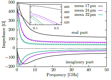
First, the (complex) impedance of the structures was simulated as a function of the frequency of the AC modulation, for a DC component equal to 2 mA. Impedance is one of the parameters measured in the SSM experiment, so it is relatively easy to compare it to the results of the experiment. Fig. 2 shows impedance spectra for the smallest mesa, the largest mesa, and one in between. The difference between the LC (dashed lines) and SC (solid lines) is not clearly apparent, especially in the imaginary part where at the scale used in the graph the curves practically overlap. In the real part, the difference between the LC and SC structures seems small, but this is only at the scale of the entire graph. At frequencies 𝑓 higher than a few GHz, where Re˜𝑍( 𝑓 ) ≪ Re˜𝑍(0) , the difference between the LC and SC structures becomes more noticeable. The importance of this difference will become more obvious in our discussion of further results.
For a modulation frequency equal to 0, Im(˜𝑍 ) = 0, while Re(˜𝑍) is the differential resistance of the laser. In the inset to Fig. 2, the differential resistance can be seen to drop moderately as the diameter of the mesa increases. The larger p-type contact surface also helps to further reduce the resistance. At high frequencies, the modulus of the impedance is lower for larger mesas. This is caused by the higher capacitances in the structures with larger oxide layer surfaces. Another indication of increased capacitance is the greater steepness of the curves for larger mesas.
The fact that impedance is lower only means that, with the same amplitude of the voltage AC component, the amplitude of the AC component of the driving current is higher. The central concern here is the impact this has on the amplitude of the modulation of light emitted by the laser. The impedance of a laser is relatively easy to verify. However, it provides only limited information. In order to investigate the impact of the electrical properties of the lasers on the modulation of emitted light, we calculate the parameter 𝐼act defined in (18). In Fig. 3, 𝐼act is shown as a function of the modulation frequency 𝑓 for the same structures as in Fig. 2. Additionally, Fig. 3(b) shows the impact of a resistance of 50Ω connected in series to the laser. In this case, the AC component of the voltage, with an amplitude of 0.1V, is applied to the laser with a resistor. The amplitude of the voltage on the laser itself is therefore lower, and decreases with frequency because the absolute value of the laser impedance also decreases.
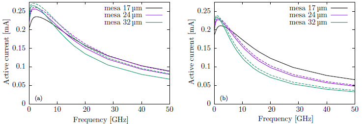
In each of the plots in Fig. 3, there are resonance peaks at low frequencies. The active currents then decrease with frequency. This effect is caused by the fact that a part of the carriers in the doped layers adjacent to the active region (or the oxidation) move up and down but do not cross the boundary with the layer with a lower conductivity (such as the junction or the insulating oxidation). Generally, the larger the mesa, the faster 𝐼act drops. This is related to the higher capacitance, which is due to the larger area of the insulating oxide layers. The lower differential resistance of the larger structures is not significant enough to counterbalance the increased capacitance.
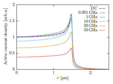
The radial distribution of the active current injected into the active region is determined by the distribution of impedance in the laser volume. At 𝑓 → 0, the impedance becomes the differential resistance. The distribution of resistance, which determines the distribution of the DC current, is not identical to the distribution of differential resistance. For this reason, in principle the profile of the active current may have a different shape to that of the DC current injected into the active region. Fig. 4 shows profiles of current density defined as 𝑗act (𝑟) = | ˜𝑗j (𝑟) |. The curves are normalised in such a way that at 𝑟 = 0 the curve for the DC current density and 𝑗act for the very low frequency of 10−3 GHz are equal to 1. This enables the shapes of the curves to be compared. The proportions between the AC profiles have been maintained. The shapes of the DC and the low-frequency AC curves are very similar, although the AC curves are slightly more uniform within the aperture (𝑟 < 1.5 μm). The uniformity improves with increasing modulation frequency.
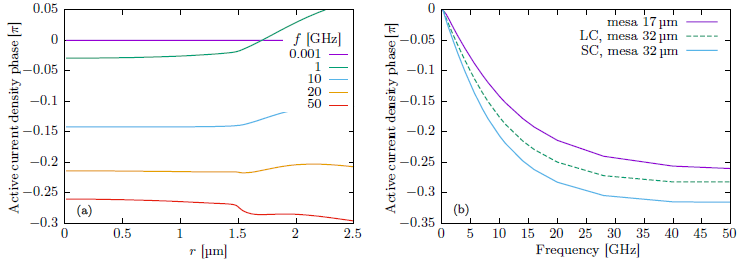
The plots in Fig. 4 do not provide information on the phase of the injected current density. Hypothetically, at the moment when the modulated current density is highest at the centre, it may be lowest near the aperture edge. Such a situation is undesirable, because it reduces the amplitude of the total number of carriers injected into the junction. Fig. 5(a) shows the lateral phase distribution of the junction voltage (equivalent to the electrical field, or active current density) phase. The phase is calculated relative to the phase of the voltage applied to the electrodes. The phase is highly uniform within the aperture. Since most of the active current is contained within the aperture, it can be approximately assumed that the whole active current has a well-defined phase, equal to the phase at the centre. This phase is shown as a function of the modulation frequency in Fig. 5(b).
When the laser is modulated with a non-sinusoidal voltage, such as when modulation is used to encode information or when eye diagrams are measured, the Fourier transform of the modulation voltage contains a wide spectrum of harmonics, from 𝑓 = 0 to frequencies higher than the bit-rate. Differences in the phase of the harmonic components of the active current will increase the horizontal blurring of eye diagrams. As shown in the case of the parameters presented in Fig. 2 and 3, the structures with a larger electrical contact perform better than their small-contact counterparts.
In textbook analyses of the SSM response of a laser, the impact of capacitance-related phenomena is usually approximated by the following first-order low-pass filter formula [14]:
\( \left(\frac{I_{\mathrm{act}}(f)}{I_{\mathrm{act}}(0)}\right)^2=\frac{1}{1+\left(f / f_p\right)^2} \) (19)
The characteristic frequency 𝑓𝑝 is simply the frequency at which the squared value of the active current is equal to half of its 0-frequency limit. This simplified approach cannot describe the non-monotonic behaviour of the 𝐼act ( 𝑓 ) curves predicted by our model. In order to define a parameter similar to 𝑓𝑝, the electric −3 dB frequency 𝑓 e 3dB is defined in the following way:
\( \left(\frac{I_{\mathrm{act}}\left(f_{3 \mathrm{~dB}}^{\mathrm{e}}\right)}{\max _f\left(I_{\mathrm{act}}(f)\right)}\right)^2=\frac{1}{2} \) (20)
Instead of using the 0-frequency limit of the active current, we use as the reference value the maximal current max𝑓( 𝐼act( 𝑓 ) ) . The reason for this is the observation that, in the analysed cases, this maximum is reached at low frequencies relative to the considered bandwidth (Fig. 3). In the SSM experiment, where the response curves are usually very noisy, this maximum can be observed easily as the 0-frequency limit. When fitted to the simulated 𝐼act ( 𝑓 ) curves, the first-order low-pass filter relation in (19) shows good resemblance at high frequencies and the fitted 𝑓𝑝 has a value similar to the corresponding 𝑓 e 3dB. In Fig. 6, 𝑓 e 3dB is shown as a function of the mesa diameter for the LC and SC structures. This plot refers to the case where no additional resistor is connected to the laser, so it corresponds with the curves in Fig. 3(a). Both curves decrease with the mesa diameter. However, the structures with a larger top contact (LC) are visibly less affected by the adverse impact of increasing the mesa diameter.
Conclusions
This article has presented a model of the dynamic electrical properties of semiconductor lasers based on the numerical solution of an appropriate PDE. The model allows for calculation of the driving voltage with a sinusoidal timedependent component. The inclusion of time-dependent phenomena is based on the use of complex values for electrical conductivity in otherwise traditional PDEs, so in principle third-party software can be used for the simulations. Unlike models based on equivalent circuits, our model allows for investigations that take into account the lateral direction.
A series of simulations was performed for GaAs-based, oxide-confined VCSEL structures with different top mesas and top electrical contact surfaces. We calculated the laser impedance as a function of time and defined a parameter called the active current, specifying the amplitude of the current that modulates the number of carriers in the active region. It was shown how this current and its phase change with increasing modulation frequency. According to the simulations, for a fixed mesa d iameter i t i s b eneficial to have a top electrical contact that is as large as possible. In order to increase the mesa, while keeping the diameter of the aperture unchanged, the surface area of the oxide layers must be increased. Increasing the mesa reduces the resistance of the laser; but in the case of a constant aperture diameter increasing the surface area of the oxide layers deteriorates laser performance at high frequencies.
The model presented here can in principle be used as a generalisation of any FEM model for electrical devices, provided that electrical inductance can be neglected. As a result, it should be relatively easy to implement, allowing for simulations of high-frequency modulations in semiconductor devices, which are extremely important components in data-transfer systems.
Authors’ statement
Research concept and theoretical model, M.W.; numerical implementation and coding, R.P.S.; testing and modelling of the laser, M.W. and R.P.S.
Acknowledgements
This work was partially supported by the Polish National Science Centre, grant no. 2016/21/B/ST7/03532 and by the Polish Ministry of Science and Higher Education, grant I-3/501/17-3-1-69.
References
-
Haghighi, N., Moser, P. & Lott, J. A. 40 Gbps with electrically parallel triple and septuple 980 nm VCSEL arrays. J. Light. Technol. 38 , 3387–3394 (2020). https://doi.org/10.1109/JLT.2019.2961931
-
Chorchos, L. et al. Energy efficient 850 nm VCSEL based optical transmitter and receiver link capable of 80 Gbit/s NRZ multi-mode fiber data transmission. J. Light. Technol. 38 , 1747–1752 (2020). https://doi.org/10.1109/JLT.2020.2970299
-
Wasiak, M. et al. Numerical model for small-signal modulation response in vertical-cavity surface-emitting lasers. J. Phys. D 53 , 345101 (2020). https://doi.org/10.1088/1361-6463/ab8b94.
-
Grabowski, A., Gustavsson, J., He, Z. S. & Larsson, A. Large- signal equivalent circuit for datacom VCSELs. J. Light. Technol. 39 , 3225–3236 (2021). https://doi.org/10.1109/JLT.2021.3064465.
-
Chang, Y. & Coldren, L. A. Efficient, high-data-rate, tapered oxide-aperture vertical-cavity surface-emitting lasers. IEEE J. Sel. Top. Quantum Electron. 15 , 704–715 (2009). https://doi.org/10.1109/JSTQE.2008.2010955.
-
Grabowski, A., Gustavsson, J., He, Z. S. & Larsson, A. Large-signal circuit model for datacom VCSELs. In 2018 IEEE International Semiconductor Laser Conference (ISLC), 1–2 (IEEE, 2018).
-
Syrbu, A. et al. 10 Gbps VCSELs with high single mode output in 1310 nm and 1550 nm wavelength bands. In OFC/NFOEC 2008, 1–3 (IEEE, 2008). https://doi.org/10.1109/OFC.2008.4528529
-
Wasiak, M. et al. Numerical model of capacitance in vertical- cavity surface-emitting lasers. J. Phys. D 49 , 175104 (2016). https://doi.org/10.1088/0022-3727/49/17/175104.
-
Griffiths, D. J. VCSEL fundamentals. In Introduction to electrody- namics, 90–96 (Prentice-Hall, 1999).
-
Wheeler, H. A. Formulas for the skin effect. Proc. IRE 30 , 412–424 (1942). https://doi.org/10.1109/JRPROC.1942.232015.
-
Wasiak, M. et al. Modelling of the modulation properties of ar- senide and nitride VCSELs. Proc. SPIE 10122 , 101220A (2017). https://doi.org/10.1117/12.2253646
-
Jun, Y. C. et al. Active tuning of mid-infrared metamaterials by electrical control of carrier densities. Opt. Express 20 , 1903–1911 (2012). https://doi.org/10.1364/OE.20.001903.
-
Wasiak, M., Sarzała, R. P. & Śpiewak, P. Influence of resonator length on performance of nitride TJ VCSEL. IEEE J. Quantum Electron. 55 , 1–9 (2019). https://doi.org/10.1109/JQE.2019.2946386
-
Michalzik, R. VCSEL fundamentals. In VCSELs: Fundamentals, Technology and Applications of Vertical-Cavity Surface-Emitting Lasers, 19–75 (Springer Berlin Heidelberg, 2013).