Digital subpixel algorithm for small pixel photon counting devices
Aleksandra Krzyżanowska1*
Piotr Otfinowski1
- Faculty of Electrical Engineering, Automatics, Computer Science and Biomedical Engineering, AGH University of Krakow, al. A. Mickiewicza 30, 30-059 Krakow, Poland
Article Info
Received 10 Sep. 2024
Received in revised form 05 Nov. 2024
Accepted 17 Nov. 2024
Available on-line 12 Dec. 2024
Keywords: charge sharing; subpixel algorithm; hybrid pixel detectors; photon counting.
Abstract
Hybrid pixel detectors are segmented devices widely used for photon detection. They consist of a sensor and readout electronics bonded together. Due to their hybrid structure, sensors of different materials can be used to register a wide range of photon energies. Moreover, the devices working in a single photon counting (SPC) mode allow registering each incoming photon separately, providing noiseless imaging. The spatial resolution of the detectors and photon count rate registered per unit area can be improved by reducing pixel size. However, small-pixel devices suffer from charge sharing. The charge sharing between pixels can be observed if the charge cloud generated in the photon-sensor event spreads due to diffusion and repulsion. Several anti-charge-sharing algorithms exist and some have been successfully implemented inside the ASICs readout. Even though they allow the allocation of the event to the proper pixel and reconstruction of the total photon energy, the detector resolution is limited by the readout channel area which must be large enough to fit the complex mixed-mode functionality. The article presents the simulations of an alternative solution which can improve both spatial resolution and high-count-rate performance. In the authors’ approach, charge sharing is regarded as a positive effect which can be used to estimate the photon interaction position with subpixel resolution. The algorithm is evaluated to improve detection efficiency and required pixel area for implementation in deep submicron technologies.
Introduction
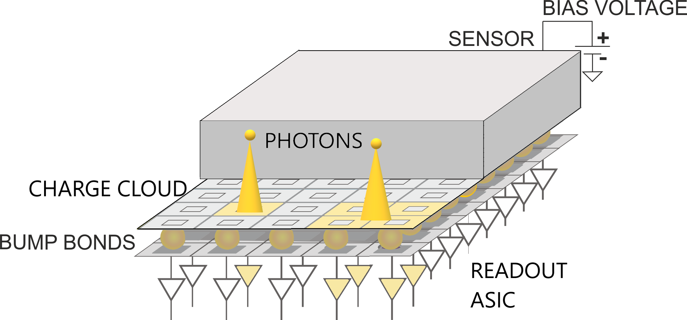
X-ray photon hybrid pixel detectors are segmented devices widely used in space, industrial, and medical applications [1]. They consist of a sensor and readout electronics bonded together which establish both mechanical and electrical connections between each detection segment and a matching readout channel. Due to their hybrid structure, sensors of different materials can be used to register a wide range of photon energies. Moreover, the devices working in a single photon counting (SPC) mode allow registering each incoming photon separately, providing noiseless imaging. The spatial resolution of the detectors and the photon count rate registered per unit area can be improved by reducing the pixel size.
However, small-pixel devices suffer from the charge sharing effect which is another cause of spatial resolution degradation [2]. Charge sharing between pixels can be observed if the charge cloud generated when a photon hits a sensor spreads due to diffusion and repulsion, as shown in Fig. 1. As a consequence, the partial signals are registered by neighbouring pixels, which results in the signal amplitudes being no longer proportional to the initial photon energy. This leads to a decrease in the counts registered within the higher energies, an increase in the false counts within lower energies in the spectrum, and a misallocation of the photon. It was studied that in detectors with a channel size of 50 × 50 μm2, charge sharing is responsible for severe disruptions in spatial resolution and energy spectrum [3].
Several anti-charge-sharing algorithms exist and some are successfully implemented inside the ASICs readout. The algorithm principles are based on charge reconstruction and assigning an event to a single pixel [4–7], pattern recognition techniques [8, 9] or searching for the centre of gravity [10]. Even though they allow the allocation of the event to the proper pixel and reconstruction of the total photon energy, the detector resolution is limited by the readout channel area which must be large enough to fit the complex mixed-mode functionality.
The first work presenting a subpixel algorithm imple-mented inside a chip is [11]. It used an asynchronous logic to detect simultaneous events in neighbouring pixels and time-over-thresholds differences to determine which subpixel should be allocated to a photon. There are also post-processing techniques for integrating detectors [12, 13] that use interpolation methods for increased resolution.
The article presents simulations of an alternative solution that can improve spatial resolution and high-count-rate performance and can be implemented on a chip. In the authors’ approach, charge sharing is a positive effect that can be used to estimate the photon interaction position with a subpixel resolution based on the proportions of charge registered by the pixel neighbourhood. Therefore, the final detector resolution will be the product of the physical channel size and the virtual pixel subdivisions.
The authors’ previous works [14–16] present a theoreti-cal approach to determine the requirements and limitations of a subpixel algorithm. In this work, the authors present design details and simulation results of the in-pixel logic circuit implementing a new subpixel algorithm based on an inter-pixel signal amplitude comparison.
Algorithm principles
Virtual pixel subdivisions
To improve the detection spatial accuracy most efficiently, it would be convenient to divide a pixel uniformly, e.g., into 2 × 2 or 3 × 3 subpixels with equal areas. However, such a division is difficult to achieve due to the nature of charge sharing. On the one hand, if a charge cloud radius is too small concerning pixel dimensions, the resulting division would result in a large subpixel near the physical pixel centre, where charge sharing does not occur, and small subpixels near the physical edges of the pixel. On the other hand, if the charge cloud radius is comparable to the pixel pitch and the charge is shared among three or more pixels, each pixel receives a small fraction of the initial charge which deteriorates the signal-to-noise ratio (SNR) and makes the division into subpixels susceptible to electronic noise and less reliable.
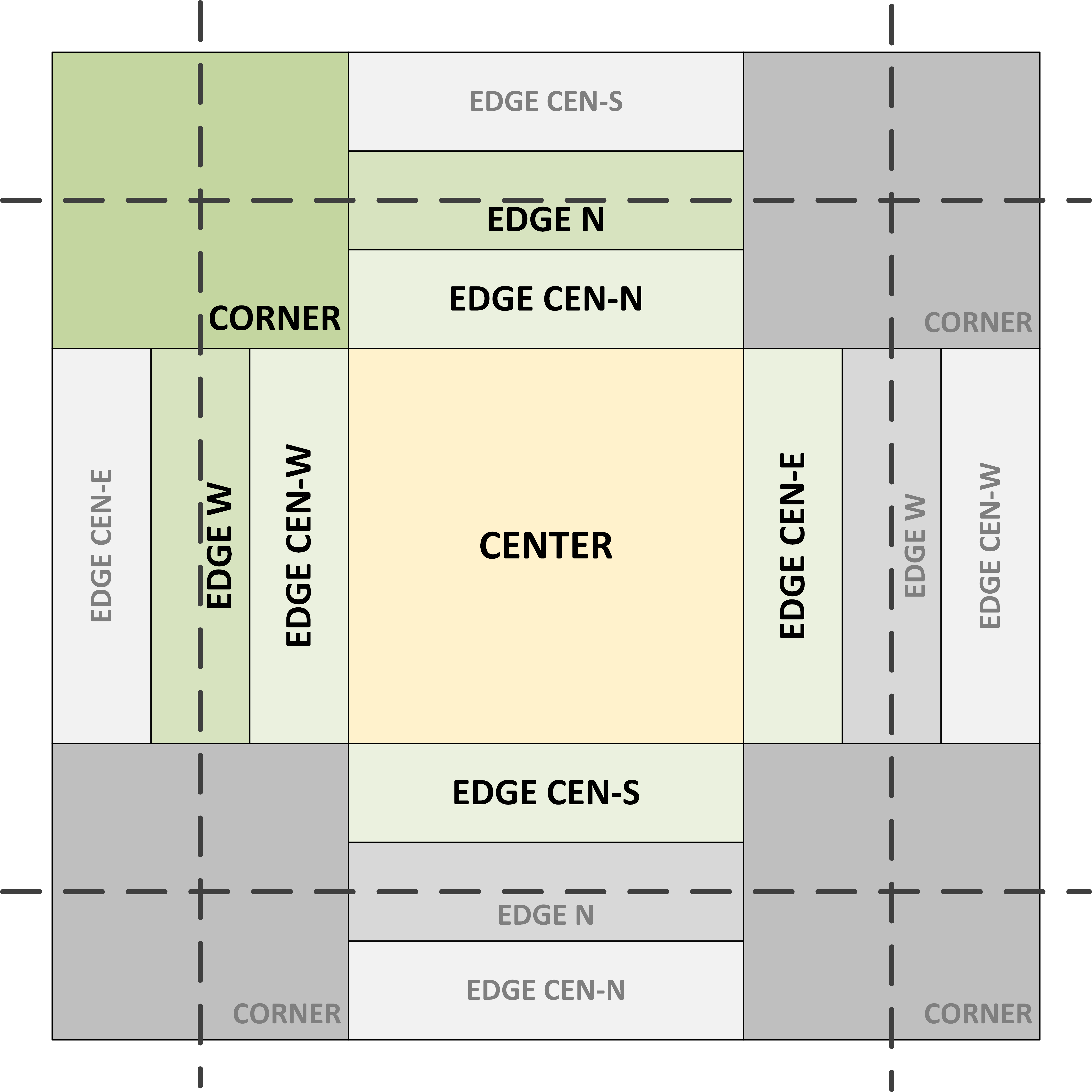
Our approach aims to achieve a compromise between the two situations described above, having in mind the realistic and achievable both the charge cloud radius and the SNR of the readout circuit. The authors propose to divide a single physical pixel into a total of eight subpixels, as depicted in Fig. 2. These subpixels are pixel centre (CENTER), four inner edges (CEN-N, CEN-W, CEN-S, CEN-E), two outer edges, shared between two physical pixels (EDGE-N and EDGE-W, shared with a neighbouring pixel in the north and west direction, respectively), and a pixel corner (CORNER), shared among four neighbouring pixels, in north, north-west, and west directions. The sizes of these subpixels are not equal and they will depend on the charge cloud radius.
Algorithm implementation
The algorithm relies on a conventional readout channel architecture. It consists of a charge sensitive amplifier (CSA) which amplifies a signal coming from a semicon-ductor detector and converts it to a voltage pulse. Then, the pulse can be either compared to a number of threshold voltages by discriminators or digitized by an analogue-to-digital converter (ADC). In this paper, the authors assume that the latter option is used.
The idea diagram of the pixel schematic is presented in Fig. 3. The algorithm is implemented in a digital domain and operates exclusively on digital signals, outputs of an in-pixel ADC. Algorithm operation is synchronous to an external clock (e.g., ADC sample clock).
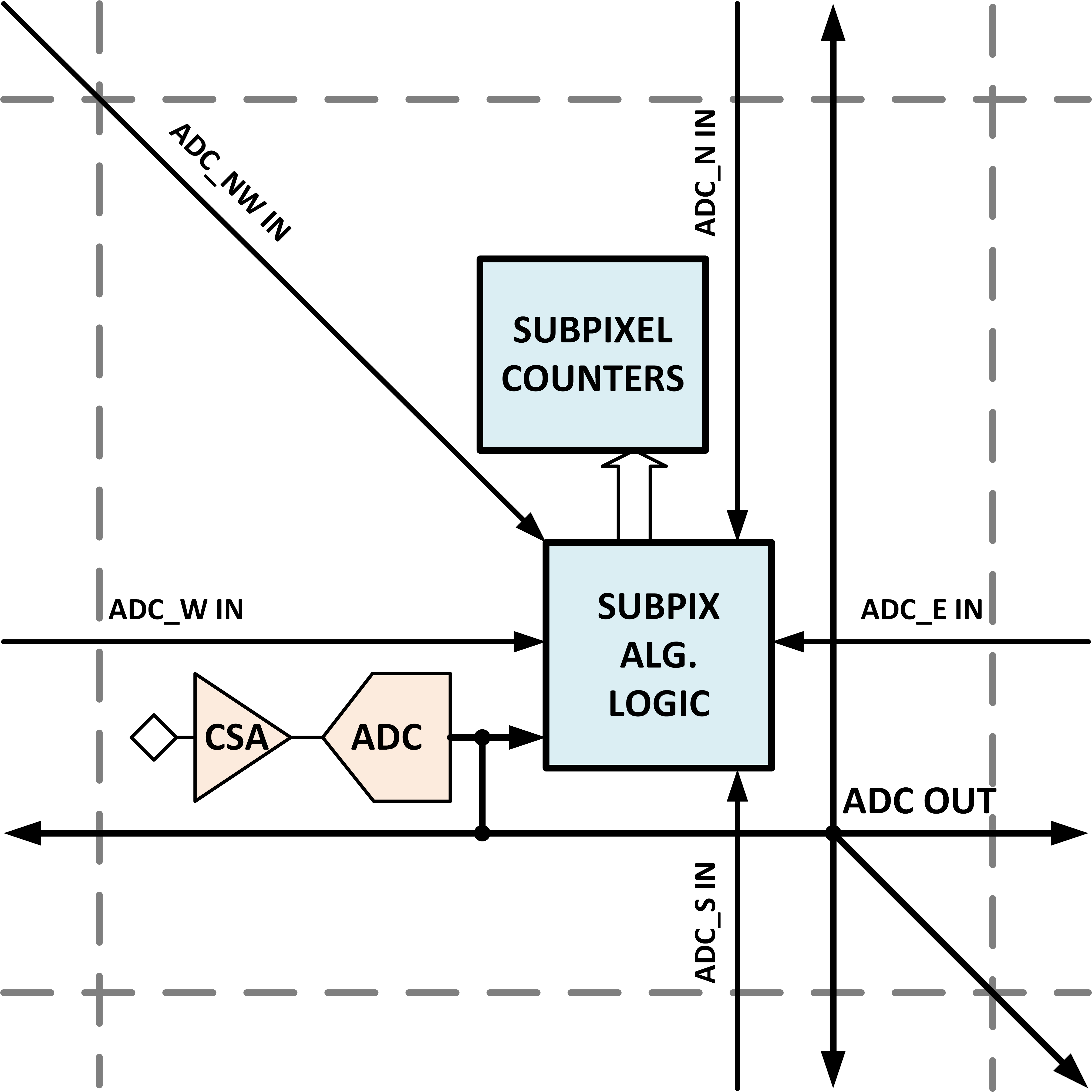
The algorithm uses ADC output from the current pixel together with ADC outputs from five neighbouring pixels in the following directions: west, north-west, north, east, and south. All incoming ADC signals are compared against two thresholds: the lower one is set just above the noise floor and the higher one is set at half of the maximum CSA pulse amplitude.
The algorithm evaluates input signals on every clock cycle. When an event is detected (i.e., ADC first crosses a threshold and then returns below it), an appropriate subpixel counter is incremented. The operation of subpixel decision logic can be described as a set of the following rules for the input signal values in a pixel:
- If any threshold was crossed in the current pixel, while none was crossed in the neighbouring pixels, an event is assigned to the centre subpixel.
- If only a low threshold was crossed in two neighbouring pixels, an event is assigned to an edge subpixel between these pixels.
- If a high threshold was crossed in the current pixel and a low threshold was crossed in one of the neighbouring pixels, an event is assigned to a corresponding inner-edge subpixel.
- If a low threshold was crossed in three or more neigh-bouring pixels, an event is assigned to a corner subpixel between these pixels.
If any of the above mentioned conditions are met, an event is assigned to a specific subpixel and a digital counter associated with the subpixel is incremented.
The decision logic rules can be summarized with the following set of equations (equations of other edge subpixels are computed analogically):
\( \begin{aligned} & \operatorname{CENTER}=\left(\mathrm{ADC} \geq \mathrm{TH}_{\mathrm{L}}\right) \cdot\left(\mathrm{ADC}_{\mathrm{N}}<\mathrm{TH}_{\mathrm{L}}\right) \cdot\left(\mathrm{ADC}_{\mathrm{W}}<\mathrm{TH}_{\mathrm{L}}\right) \\ & \cdot\left(\mathrm{ADC}_{\mathrm{S}}<\mathrm{TH}_{\mathrm{L}}\right) \cdot\left(\mathrm{ADC}_{\mathrm{E}}<\mathrm{TH}_{\mathrm{L}}\right) \cdot\left(\mathrm{ADC}_{\mathrm{NW}}<\mathrm{TH}_{\mathrm{L}}\right) \\ & \mathrm{EDGE}_{\mathrm{W}}=\left(\mathrm{TH}_{\mathrm{H}}>\mathrm{ADC} \geq \mathrm{TH}_{\mathrm{L}}\right) \cdot\left(\mathrm{TH}_{\mathrm{H}}>\mathrm{ADC}_{\mathrm{W}} \geq \mathrm{TH}_{\mathrm{L}}\right) \\ & \cdot\left(\mathrm{ADC}_{\mathrm{N}}<\mathrm{TH}_{\mathrm{L}}\right) \cdot\left(\mathrm{ADC}_{\mathrm{S}}<\mathrm{TH}_{\mathrm{L}}\right) \cdot\left(\mathrm{ADC}_{\mathrm{NW}}<\mathrm{TH}_{\mathrm{L}}\right) \\ & \mathrm{EDGE}_{\mathrm{CEN}-\mathrm{W}}=\left(\mathrm{ADC} \geq \mathrm{TH}_{\mathrm{H}}\right) \cdot\left(\mathrm{ADC}_{\mathrm{W}} \geq \mathrm{TH}_{\mathrm{L}}\right) \\ & \cdot\left(\mathrm{ADC}_{\mathrm{N}}<\mathrm{TH}_{\mathrm{L}}\right) \cdot\left(\mathrm{ADC}_{\mathrm{S}}<\mathrm{TH}_{\mathrm{L}}\right) \\ & \text { CORNER }=\left(\mathrm{ADC} \geq \mathrm{TH}_{\mathrm{L}}\right) \\ & \cdot\left(\left(\mathrm{ADC}_{\mathrm{N}} \geq \mathrm{TH}_{\mathrm{L}}\right) \cdot\left(\mathrm{ADC}_{\mathrm{W}} \geq \mathrm{TH}_{\mathrm{L}}\right)+\left(\mathrm{ADC}_{\mathrm{NW}} \geq \mathrm{TH}_{\mathrm{L}}\right)\right) \end{aligned} \) (1)
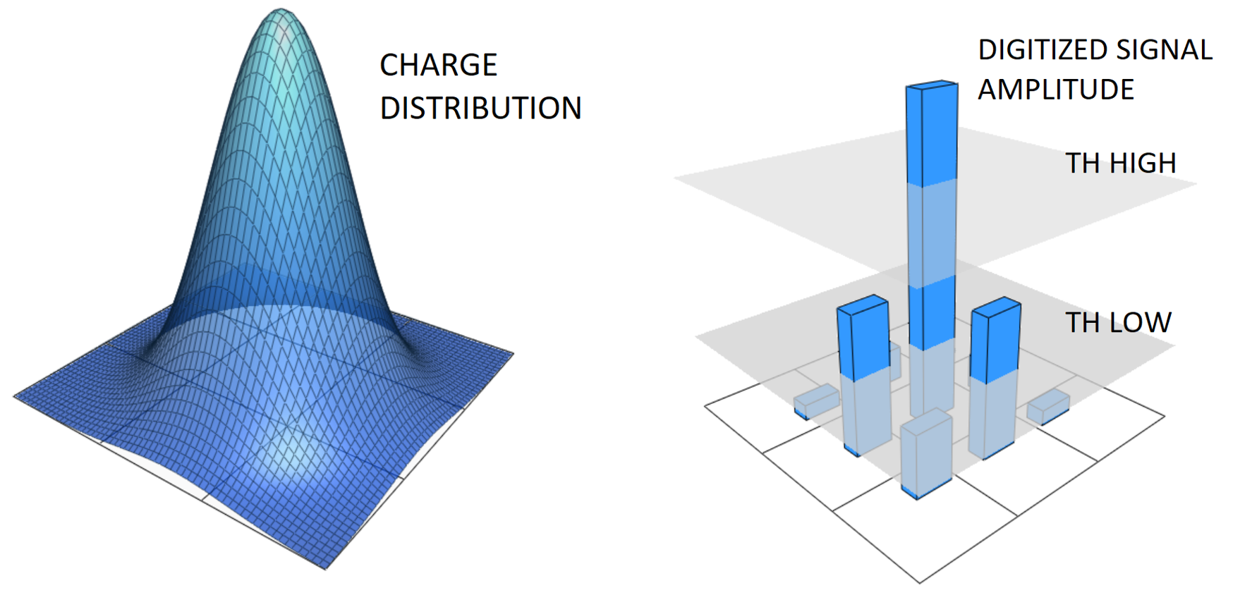
An example of an event where the charge was shared among many pixels is visualized in Fig. 4. The digitized signal in each pixel is compared to two thresholds and the results become the input signals for the algorithm decision logic. Then, the ADC values in each pixel are compared with the ADC values of neighbouring pixels. In the presented case, an event is assigned to the corner subpixel.
Algorithm simulations
Simulation setup
The complete simulation setup was prepared using the SystemVerilog hardware description language. The algorithm logic was modelled by a synthesizable register transfer level (RTL) module whose operation principle was described in section 2. A simplified model was prepared for pixel analogue front-end (AFE) electronics, also in the SystemVerilog language. Such an approach allowed the authors’ to carry out simulations entirely in a digital simulator. Cadence Xcelium was used for that purpose.
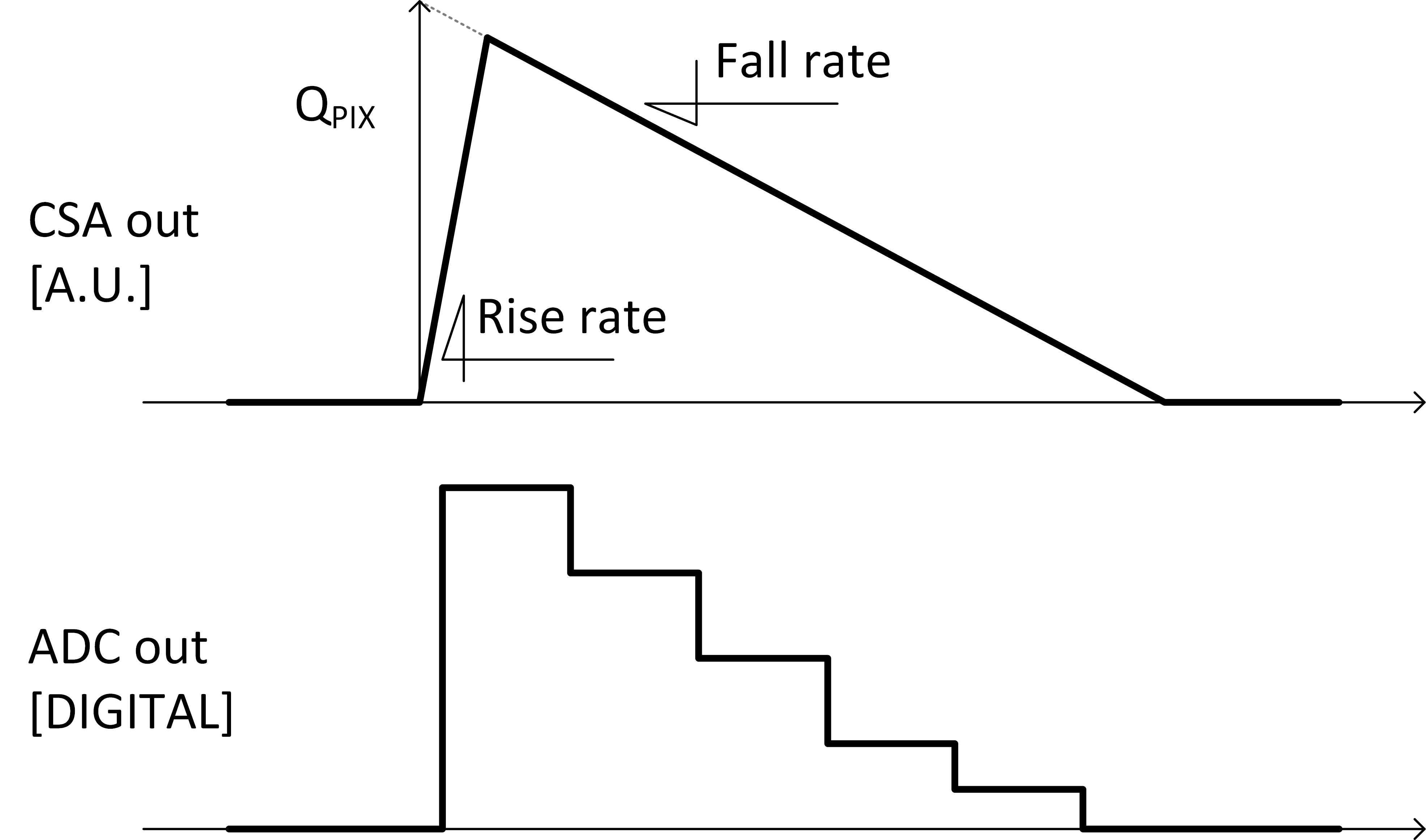
AFE model had a readout channel architecture consisting of a charge sensitive amplifier together with an in-pixel ADC. CSA model assumed a triangular output voltage pulse (linear discharge, Fig. 5) with variable parameters like gain, noise, rise-rate and fall-rate, together with dispersion of these parameters among pixels. CSA output signal is then digitized in each pixel by an ADC. Its model allowed to vary parameters such as resolution, full-scale range, sample rate, and nonlinearity.
The testbench consisted of an array of 3 × 3 pixels, each containing AFE model and subpixel algorithm logic. Such size was sufficient to verify algorithm operation, as inter-pixel communication reaches only eight pixels in the immediate neighbourhood. Thus, the pixel located in the middle of the array allows the testing of all possible interactions between pixels.
Charge can be deposited in a selected array area, simu-lating a photon hitting the detector. Each pixel is assigned a fraction of the total charge according to the Gaussian charge distribution model and the specified charge cloud radius [14]. Then, AFE processes the charge generating stimuli for the subpixel algorithm.
Simulation procedure
To assess the allocation accuracy of the presented algorithm, a positional scan was performed. The charge was deposited at a given position a selected number of times to collect meaningful statistical data. The number of registered events by each subpixel of all pixels was stored. Then, the position of charge deposition was moved to the next location and the procedure was repeated. By scanning across the pixel array, a two-dimensional plot can be constructed, showing to which subpixel an event is assigned depending on its position.
For a single event registration, the algorithm uses ADC output from the current pixel and ADC outputs from five neighbouring pixels. An event occurring in another pixel is analogous, only shifted. Therefore, in the simulations, the scanned area was limited to one central pixel and edges and corners of its eight neighbours. The procedure was repeated for multiple charge cloud radii, ranging from 5% to 50% of the pixel pitch.
All parameters of the AFE model are summarized in Table 1.
Table 1.
AFE model parameters.
Parameter |
Value |
Charge |
2400 e− |
Charge cloud (σ) |
5%–50% pixel pitch |
Equivalent noise charge (ENC) |
50 e− |
Peaking time |
30 ns |
Pulse width |
300 ns |
ADC resolution |
5 bits |
ADC range |
3200 e− |
ADC sample rate |
20 MS/s |
Threshold low |
300 e− |
Threshold high |
1200 e− |
Simulation results
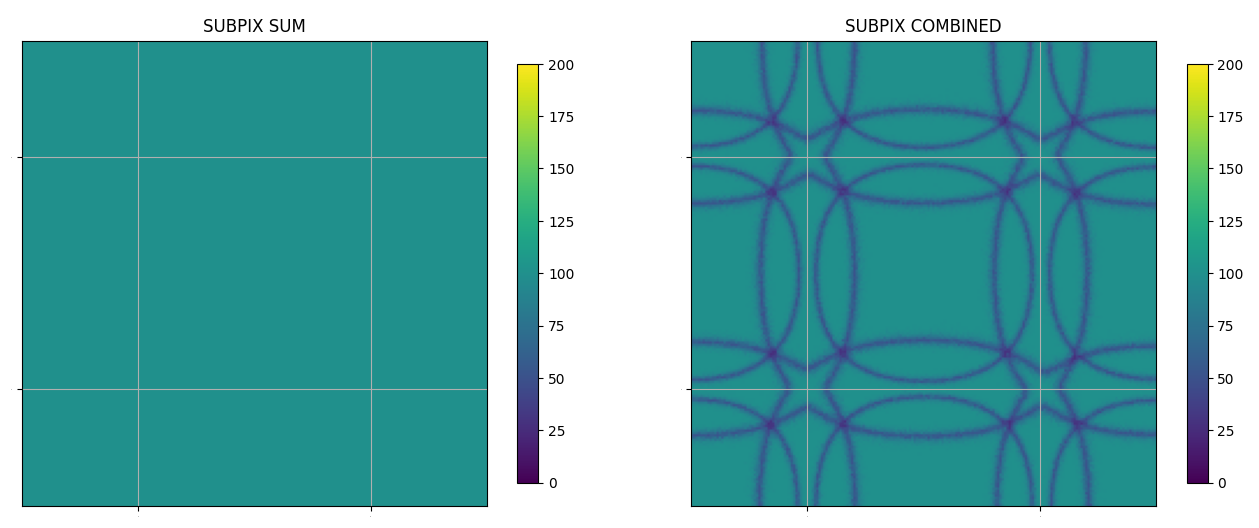
The simulation results of the position scan are presented in Figs. 6-8 as follows: the SPC_LOW / SPC_HIGH show the number of registered events by a single central pixel generated at a given location. SUM plots show the total number of events registered by all pixels referred to the event location. The COMBINED plots show the number of events registered by a pixel with the highest event count at that location. In all cases, the number of events is calculated as a % of the total number of events generated at a given location. The charge cloud radius was equal to 35% of the pixel pitch which corresponds to a detector with a 50 μm pixel pitch and a thickness of approximately 1 mm.
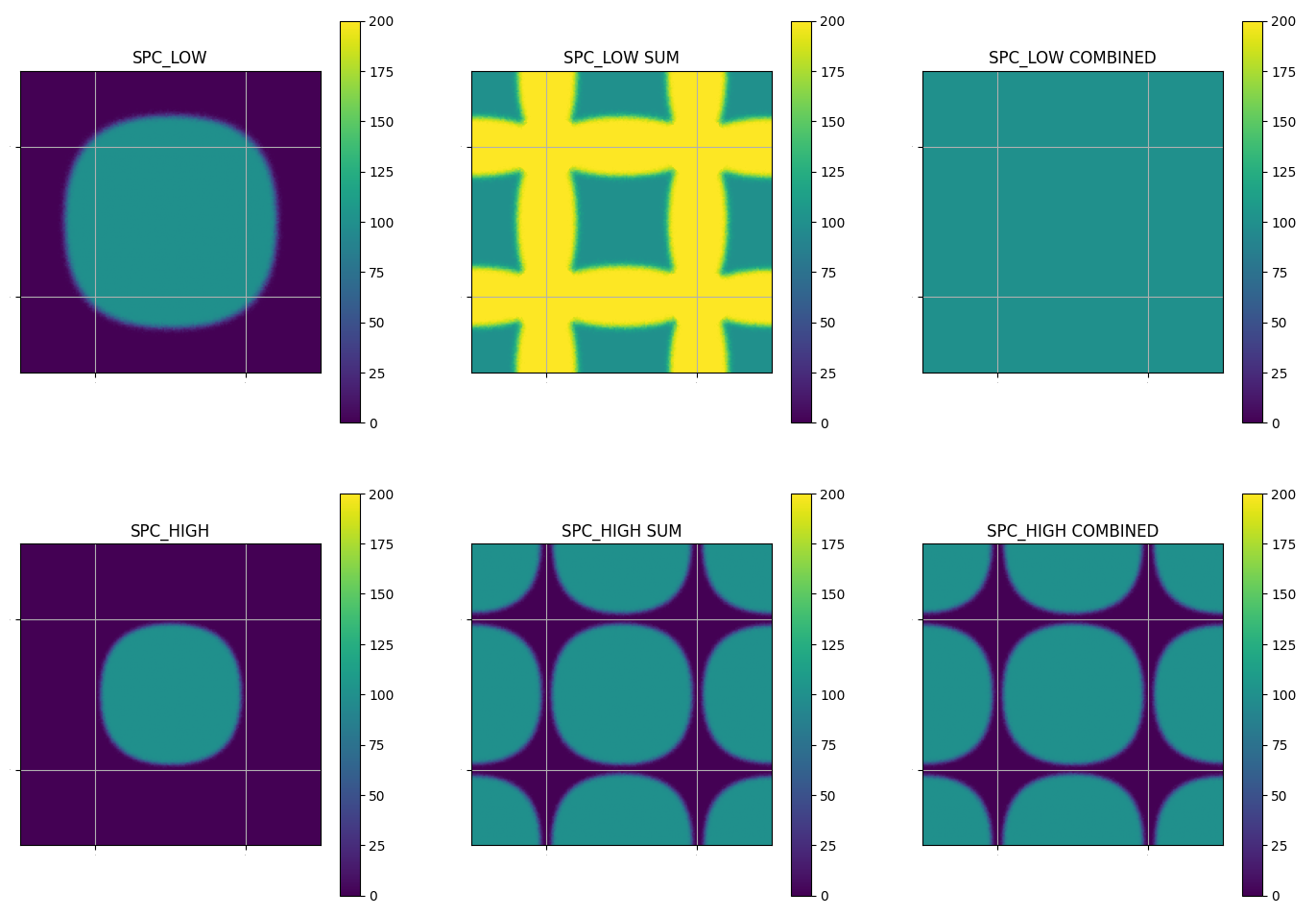
Fig. 6 presents the results of the conventional single photon counting algorithm. One can clearly see the extent of charge sharing for low threshold where sensitivity areas of adjacent pixels overlap resulting in overcounting. On the other hand, for a high threshold, there are large areas near the pixel borders where incoming photons are missed because the pulse amplitude does not cross the threshold in any of the pixels.
Fig. 7 presents the position scan of the proposed algorithm. The eight plots presented correspond to subpixels of the central pixel. While the central subpixel has the largest area, other subpixels also register many incoming photons.
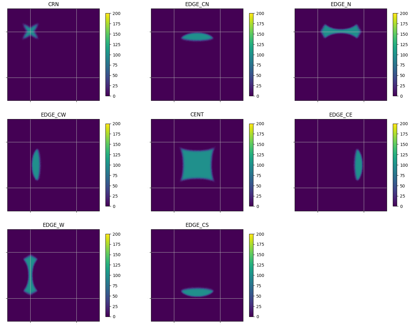
Fig. 8 shows the cumulative subpixels from all pixels. A pixel-centric ring can be observed which follows the range of charge sharing for two thresholds and subpixels are obtained by subtraction or cross-section of these areas originating from neighbouring pixels. It can be seen that the sum of counts from all subpixels is equal to the sum of generated events without losing or double counting.
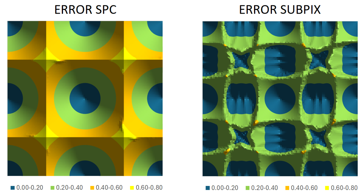
The allocation error was defined as a criterion to characterise allocation accuracy in the SPC and subpixel modes. The Euclidian distance between the simulated event positions and centres of pixels or subpixels allocating the event was calculated and plotted as a function of the hit position.
The allocation error vs. the hit position is presented in Fig. 9. Average error for all the event positions is equal to 0.38 in SPC mode and 0.21 in subpixel mode, respectively. The highest values of error, reaching 0.7, are present as expected in the pixel corners in the SPC mode. The lower average error value in the subpixel mode indicates better spatial resolution.
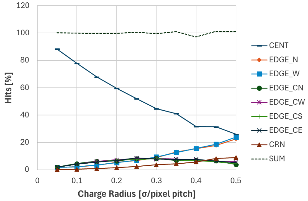
Finally, Fig. 10 shows a dependency between the charge cloud radius and the fraction of registered events assigned to each subpixel among all events registered by the pixel. It can be observed that the centre subpixel dominates up to a charge cloud radius equal to 25% of the pixel pitch, which accounts for more than half of the total registrations. Over that point, the presented subpixel algorithm would provide substantial improvement in photon detection spatial accuracy.
Conclusions
The authors presented a concept and simulation of an allocation algorithm dedicated to single-photon counting pixel detectors which aims to improve spatial allocation accuracy by dividing a pixel into eight subpixels. Compared to previous work [11], it has improved the inter-pixel communication, including two thresholds and an optimized subpixel layout which yields a more uniform number of counts per subpixel. Moreover, the presented approach relies solely on pulse amplitude, in contrast to [11], which combined both pulse amplitude and time-over-threshold comparison. The main advantage is better uniformity across the whole pixel array resulting from the fact that correction of pulse amplitude is easier to implement than correction of its length [17].
The algorithm operates in the digital domain and can be easily adapted for conventional detection systems. The approximate size of the logic cell area is 45 μm2 in a CMOS 40 nm technology, making it suitable for readout circuits with a small pixel pitch.
The simulation results show that the algorithm main goal was to divide a physical pixel into smaller subpixels. That implies that increasing the spatial resolution of the pixel detector by using the charge sharing effect is possible.
Acknowledgements
This work was supported by the National Science Centre, Poland, under Contract no. UMO‑2018/29/N/ST7/02770.
References
-
X-ray Photon Processing Detectors: Space, Industrial, and Medical Applications. (eds. Hansson, C. & Iniewski, K.) 1–292 (Springer, 2023).
-
Krzyzanowska, A. Charge Sharing in Single-Photon-Counting Detectors. in X-ray Photon Processing Detectors: Space, Industrial, and Medical applications (eds. Hansson, C. & Iniewski, K.) 27–38 (Springer, 2023). https://doi.org/10.1007/978-3-031-35241-6_2
-
Nilsson, H. E., Dubaric, E., Hjelm, M. & Bertilsson, K. Simulation of Photon and Charge Transport in X-Ray Imaging Semiconductor Sensors. in Nuclear Instruments and Methods in Physics Research, Section A: Accelerators, Spectrometers, Detectors and Associated Equipment 487, 151–162 (North-Holland, 2002)
-
Ballabriga, R., Campbell, M., Heijne, E. H. M., Llopart, X. & Tlustos, L. The Medipix3 Prototype, a Pixel Readout Chip Working in Single Photon Counting Mode with Improved Spectrometric Performance. in 2006 IEEE Nuclear Science Symposium Conference Record 54, 1824–1829 (IEEE, 2007). https://doi.org/10.1109/TNS.2007.906163
-
Krzyzanowska, A., Deptuch, G. W., Maj, P., Grybos, P. & Szczygiel, R. Characterization of the Photon Counting CHASE Jr., Chip Built in a 40-nm CMOS Process With a Charge Sharing Correction Algorithm Using a Collimated X-Ray Beam. in IEEE Trans. Nuclear Sci. 64, 2561–2568 (2017). https://doi.org/10.1109/TNS.2017.2734821
-
Deptuch, G. W. et al. VIPIC IC – Design and Test Aspects of the 3D Pixel Chip. in IEEE Nuclear Science Symposium Conference Record 1540–1543 (2010). https://doi.org/10.1109/NSSMIC.2010.5874034
-
Bellazzini, R. et al. PIXIE III: a very large area photon-counting CMOS pixel ASIC for sharp X-ray spectral imaging. J. Instrum. 10,C01032 (2015). https://doi.org/10.1088/1748-0221/10/01/C01032
-
Maj, P., Baumbaugh, A., Deptuch, G., Grybos, P. & Szczygiel, R. Minimization of Charge Sharing Effect in Silicon Hybrid Pixel X- Ray Detectors Based on Pattern Recognition Algorithm. in 2012 IEEE International Conference on Industrial Technology 551–556 (IEEE, 2012).
-
Otfinowski, P., Deptuch, G. W. & Maj, P. FRIC–a 50 μm pixel-pitch single photon counting ASIC with pattern recognition algorithm in 40 nm CMOS technology. J. Instrum. 15, C01016 (2020). https://doi.org/10.1088/1748-0221/15/01/C01016
-
Otfinowski, P., Deptuch, G. W. & Maj, P. Asynchronous approximation of a center of gravity for pixel detectors’ readout circuits. IEEE J. Solid-State Circuits 53, 1550–1558 (2018) https://doi.org/10.1109/JSSC.2018.2793530
-
Otfinowski, P. et al. Increasing the position resolution in single photon counting pixel readout IC by real-time interpixel communications. IEEE Trans. Circuits Syst. II: Express Br. 71, 3695–3699 (2024) https://doi.org/10.1109/TCSII.2024.3372884
-
Cartier, S. et al. Micron resolution of MÖNCH and GOTTHARD, small pitch charge integrating detectors with single photon sensitivity. J. Instrum. 9, C05027 (2014). https://doi.org/10.1088/1748-0221/9/05/C05027
-
Chiriotti, S. et al. High-spatial resolution measurements with a GaAs:Cr sensor using the charge integrating MÖNCH detector with a pixel pitch of 25 μm. J. Instrum. 17, P04007 (2022). https://doi.org/10.1088/1748-0221/17/04/P04007
-
Krzyżanowska, A. & Szczygieł, R. Simulation study on improving the spatial resolution of photon-counting hybrid pixel X-ray detectors. Opto-Electron. Rev. 29, 187–191 (2021). https://doi.org/10.24425/opelre.2021.139756
-
Krzyzanowska, A., Niedzielska, A. & Szczygieł, R. Charge sharing simulations for new digital algorithms achieving subpixel resolution in hybrid pixel detectors. J. Instrum. 15, C02047 (2020). https://doi.org/10.1088/1748-0221/15/02/C02047
-
Krzyżanowska, A. et al. Charge sharing simulations and measurements for digital algorithms aiming at subpixel resolution in photon counting pixel detectors. J. Instrum. 18, C02024 (2023). https://doi.org/10.1088/1748-0221/18/02/C02024
-
Krzyżanowska, A., Gryboś, P., Szczygieł, R. & Maj, P. Testing multistage gain and offset trimming in a single photon counting IC with a charge sharing elimination algorithm. J. Instrum. 10, C12003 (2015). https://doi.org/10.1088/1748-0221/10/12/C12003