A camera for scanning objects in motion based onan integrated detection system working in on-chip TDI mode
Mirosław Żołądź1*
- Department of Measurement and Electronics, AGH University of Krakow, al. Mickiewicza 30, 30-059 Kraków, Poland
Article Info
Received 17 Oct. 2024
Received in revised form 22 Nov. 2024
Accepted 28 Nov. 2024
Available on-line 20 Dec. 2024
Keywords: X-rays; application-specific integrated circuit; single-photon counting; time domain integration.
Abstract
The paper presents an X-ray camera for testing moving objects. A typical application of such cameras is scanning products on an industrial production line. Currently, the most popular device detecting radiation in this type of camera consists of a pixel line based on scintillator detectors. Unfortunately, increasing its resolution automatically involves reducing the pixel size and reducing the signal-to-noise ratio. This is where the time domain integration method comes in handy, increasing the resolution without degrading the signal-to-noise ratio. The camera presented in this paper is based on an application-specific integrated circuit dedicated to this purpose. The application-specific integrated circuit core is a pixel matrix operating in a single-photon counting mode. Its architecture was designed to implement the time domain integration method and construct high-resolution cameras with a large scanning area. The article also describes the hardware and software of the application-specific integrated circuit readout system.
Introduction
X-ray imaging
X-ray imaging is used in several fields, including physics, biology, and medicine. Initially, indirect photon detection imaging was employed. This method uses panels comprising a scintillation screen and an array of photosensitive pixels [1]. The screen converts X-rays into visible light, while the array converts visible light into digital form. Unfortunately, recording the energies necessary for non-destructive testing necessitates an increase in the thickness of the screen, which, in turn, results in a reduction in the resolution of the recorded image due to the scattering of photons on the screen polycrystals.
Hybrid pixel detectors
The use of direct hybrid pixel detectors [2–5] allows for better resolution. In such detectors, a photon entering a given region of the detector deposits its energy there, generating electron-hole pairs. Applying a polarizing voltage to the electrodes of the detector creates an electric field that causes the charge carriers to move to the corresponding electrodes. As a result of the movement of electrons and holes on the detector electrodes, a current is induced until all the charges are collected.
Charge integration
Two principal techniques are employed for processing current pulses in direct detection. The older method is based on the integration of charge. In this method, charge packets induced by photons over a specified time interval are accumulated in analogue memories, such as capacitors or potential wells, within pixels. Unfortunately, besides the charges corresponding to the photons, this method also accumulates noise and fluctuations in the detector signal, resulting in a reduced image quality. Furthermore, the accumulation process inevitably results in a loss of information regarding the energy of individual photons. The analogue-to-digital conversion is conducted outside the pixels, allowing for the use of relatively small pixels (up to 10 μm × 10 μm). However, this approach necessitates the transfer of accumulated charges through the pixel which constrains the pixel matrix readout frame rate. It is important to note that the technique can withstand relatively high radiation fluxes due to its main principle, namely the integration of charges.
Single-photon counting
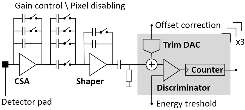
A more recent method of current pulse processing, desig-nated as single-photon counting, entails the enumeration of current pulses that align with photon strikes. A charge-sensitive amplifier converts the current pulses into voltage pulses which are then compared with a voltage threshold in a discriminator. A digital counter accumulates the discriminator digital pulses over a specified time interval. This process effectively eliminates the noise and signal fluctuations generated by the detector. Furthermore, the loss of information regarding the energy of photons can be circumvented by employing a set of discriminators (and counters) with distinct voltage thresholds [6–8]. However, it is essential to acknowledge that because analogue-to-digital conversion occurs at the pixel level, this method results in a higher minimum pixel size and a lower allowable radiation flux than the charge integration method. The latter limitation is due to the stacking effect of overlapping successive current pulses.
Detector material
In the case of hybrid pixel detectors, the manufacturing process of detectors and application-specific integrated circuits (ASICs) for current pulse processing can proceed separately, allowing to develop them independently and use different types of detectors with the same readout electronics. A material for a solid-state detector should possess the following characteristics [9–11]:
- significant signal in response to the energy deposited by the particle/photon (a small energy bandgap is required),
- low atomic number Z and low density in the case of tracking applications for particle physics experiments,
- high atomic number Z and high density in the case of X-rays for medical imaging applications,
- high carrier mobility and no trapping effects to collect all the generated charge in a short time,
- long carrier lifetime to increase the so-called charge collection efficiency,
- low leakage current at room temperature,
- large and high-quality crystals to produce a large area detector and stable and mature industrial fabrication.
Among various materials used to build a pixel sensor, the most commonly used are Si, Ge, GaAs, CdTe, CZT. Silicon sensors are very popular in high-energy physics experiments and low-energy X-ray imaging applications. However, medical applications, which usually use high X-ray energies, prefer materials with high atomic numbers, such as high-purity germanium and compound semicon-ductors (such as GaAs, CdTe, CZT).
Interconnections
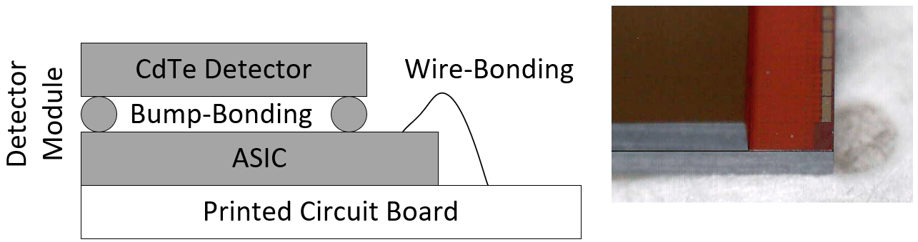
The connection between the detector pixel and the readout circuit (an integrated circuit, in practice) is made by micro-bump bonding. Beads (e.g., of tin or gold) are applied to the detector pixels and the integrated circuit pixels, then bonded at elevated temperature and pressure.
Connections between the ASIC and the detector module board (see next section) are usually made using a wire-bonding technique. The critical interconnections were concentrated on a single edge of the ASIC, enabling the placement of detector modules in a side-by-side configura-tion. This approach is essential for the development of wide-area detectors [12].
Moving objects imaging
Line detectors
Images captured by the line detector, comprising a series of pixels arranged in a row, are combined to create a single continuous image representing a sequence of moments in time. However, this approach presents a trade-off: increasing the detector spatial resolution reduces the image signal-to-noise ratio (SNR). The reduction in pixel size results in a corresponding decrease in the number of photons that reach the pixel per unit time, given a constant irradiance. Line detectors are typically based on indirect photon detection which limits their spatial resolution to 0.4 mm.
TDI method
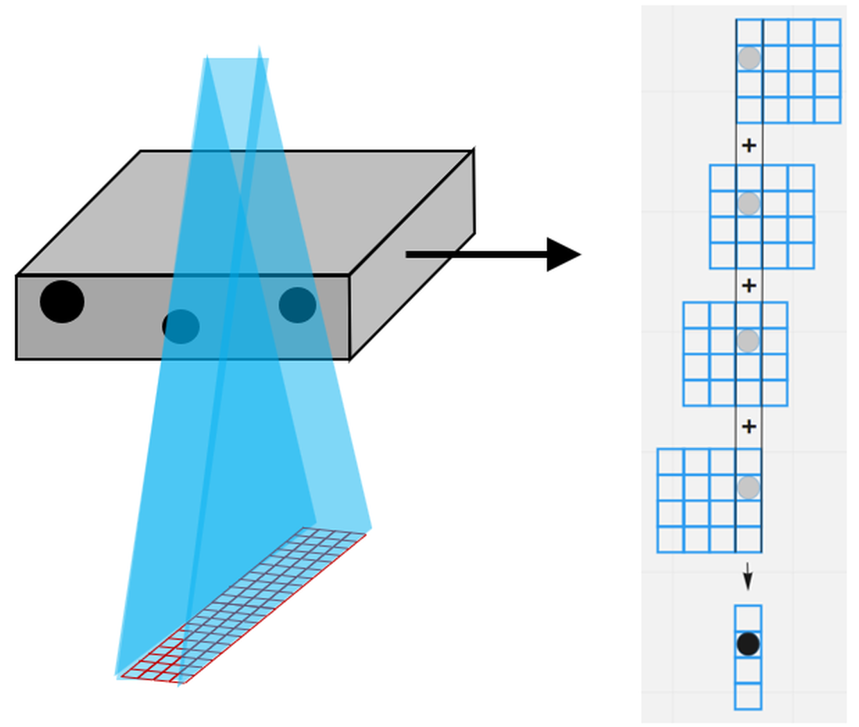
A two-dimensional sensor, specifically a pixel array, is recommended to overcome the limitation above. This approach allows for a more efficient use of the radiation flux. To obtain a continuous and sharp image of a moving object, it is necessary to employ a time domain integration (TDI) [13]. The TDI method entails the summation of images of a moving object captured at disparate sequential time points (Fig. 1). To compensate for the object motion, images must be shifted accordingly before summation. The image noise will be reduced proportionately to the square root of the number of summed images. This approach is considerably more data-intensive than a straightforward row merge for a linear detector. This is due to the necessity of reading and processing data from the entire array. Furthermore, due to the inhomogeneity of the detector and the presence of inoperative pixels, image normalization and correction of the inoperative pixels must be performed before image accumulation.
TDI on-chip method
To reduce the volume of data and the requisite computing power, a method known as on-chip TDI (on-chip integration) can be employed [14–15]. This approach leverages the fundamental capability of a single-photon counting channel, namely the accumulation of photon counts. The signal processing channel of a typical ASIC for a single-photon counting typically comprises a charge amplifier, a pulse shaping circuit, one or more discriminators, and a counter connected to each discriminator (Fig. 2). The discriminator function is to convert analogue pulses into digital pulses, but only those with an amplitude above a preset threshold. Using two or more discriminators with different discrimi-nation thresholds makes it possible to distinguish photons corresponding to different energy ranges. The counters of individual pixels can be reconfigured into shift registers to read the number of counts from the pixel array. This is the key to the TDI on-chip method, which relies on shifting the contents of the counters along the direction of object movement, with the speed of the shifting counters having to be equal to the speed of the object image. In the TDIs on-chip method, only the final row of pixels is read rather than reading the entire matrix for each pixel shift of the object. This is feasible because if the shift of the rows is synchronized with the object movement, the matrix last row accumulates photon counts corresponding to a single point of the object throughout the entirety of the object movement over the matrix. In other words, the final pixel in each column gathers counts from other pixels in the column that correspond to each phase of the object movement. It is crucial to note that the amplitude of the signal corresponding to the object is proportional to the number of rows in the matrix, as all pixels are used to obtain the image. Furthermore, the reduced volume of data read from the matrix is proportional to the number of matrix rows. It is also important to note that, from the perspective of commercial applications, the operation of photon accumulation in a direction parallel to the object motion makes the TDI on-chip method immune primarily to the presence of so-called bad pixels.
Detector module
The primary component of the camera presented in this paper is a detector module illustrated in Fig. 3. The detector module consists of a CdTe detector and an ASIC. The material, CdTe, and a thickness of the detector of 0.75 mm were selected to register radiation within the range used for food scanning. The central component of the ASIC is a matrix comprising 192-pixel columns of 64 pixels each. Dimensions of a single pixel are 100 μm × 100 μm. The chip was manufactured using a 130 nm technology, which permits the use of eight layers of metals.
ASIC
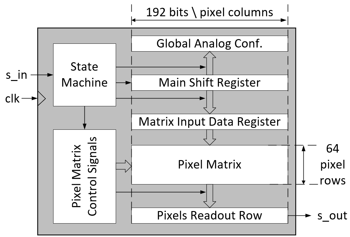
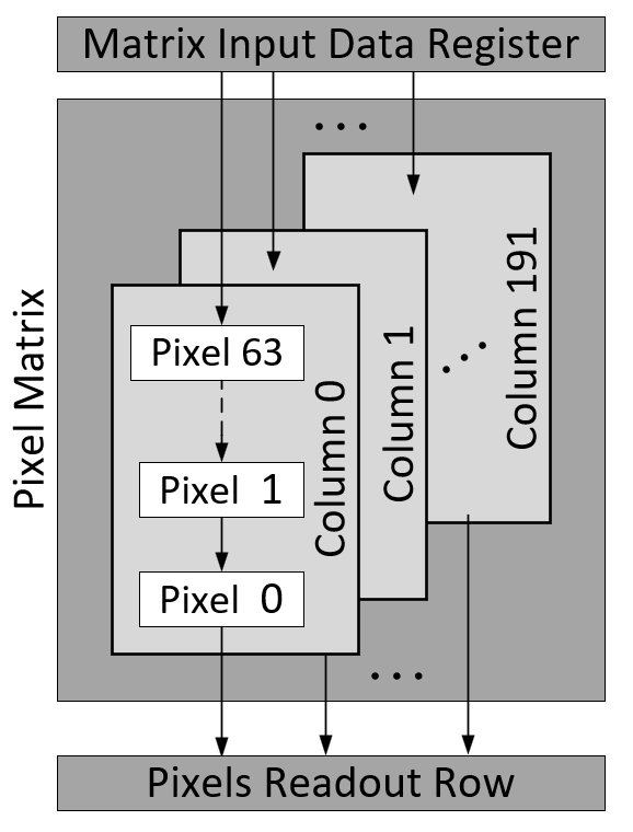
Fig. 4 shows the block diagram of the ASIC. It is designed for the on-chip TDI. Its main component is a matrix of pixels of which (i.e., pixels) a simplified schematic is shown in Fig. 2. The reading of counts from the pixels is carried out via an additional “pixels readout row”. Its task is not to count photons but to minimize the “dead” time. The “dead” time is when photons cannot be counted due to the counter reading. The counter values of all rows are continuously shifted by one row towards an additional pixel readout row which is then read outside the ASIC. The rate at which the rows are moved is adjusted to the speed of the object movement and the counters are also turned on while the additional row of pixels is being read. This solution also allows data transmission evenly distributed in time, reducing the required chip clock frequency [15]. Fig. 5 shows a schematic of part of a digital pixel array. It consists of 192 columns, each with 64 pixels. Resetting the counters in the first row of the matrix (i.e., entering ones, since the counters count “down”) and setting the operating parameters of the photon counting channel are done via the “matrix data register”.
Camera
Detector module board
Fig. 6 shows a block diagram of the camera. Its most important components are detector module boards (Fig. 7). Their task is to provide the appropriate operating conditions for the detector module. This involves: providing power supply voltages (two to the digital part and three to the analogue part of the ASIC), supplying the voltage that polarizes the CdTe detector (−300 V), and dissipating heat (about 2 W). The board is also responsible for routing the signals used to communicate with the ASIC (Fig. 4). As shown in Fig. 8, the width of the board is less than the length of the detector module, allowing a continuous plane to be formed by stacking individual modules side by side.
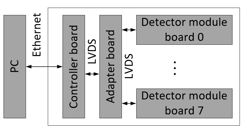
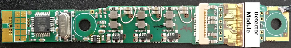
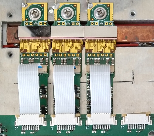
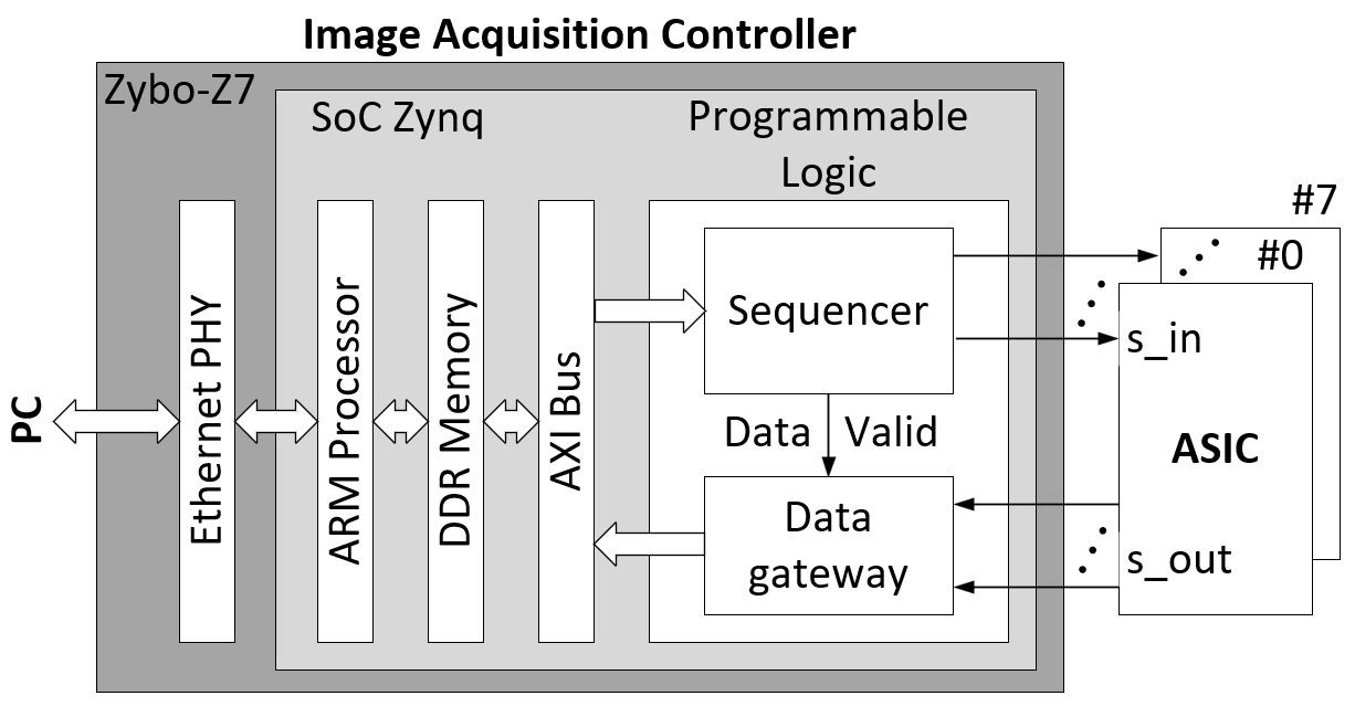
Image acquisition controller
The image acquisition controller (Fig. 9) controls data acquisition from the ASICs. Its main component is a system-on-chip (SoC). It consists of programmable logic, a processor, and shared memory. The task of the program-mable logic is to generate sequences that control the ASICs in a strict time regime and to read data from the ASICs. This data is then transferred to memory shared with the processor. Finally, processor sends the mentioned data to the PC via a 1 Gbit Ethernet interface.
Camera software
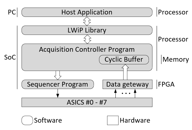
Fig. 10 shows a schematic of the system software. The host application generates a microcode for the sequencer (a dedicated programmable automaton) and then sends it, i.e., the microcode, to the said sequencer via the acquisition controller program. As a result, the sequence controlling the ASIC is generated and the measurement data, i.e., photon counts, are read from it. These data first go to a cyclic buffer (continuous reading) implemented in the SoC shared memory. From there, the controller main program sends them to the host application. The host application and the acquisition controller program communicate via a transmission control protocol (TCP) using the lightweight IP (LwIP) library.
Test measurements
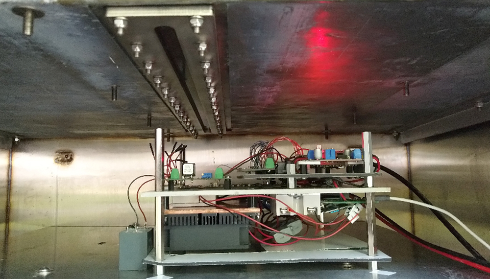
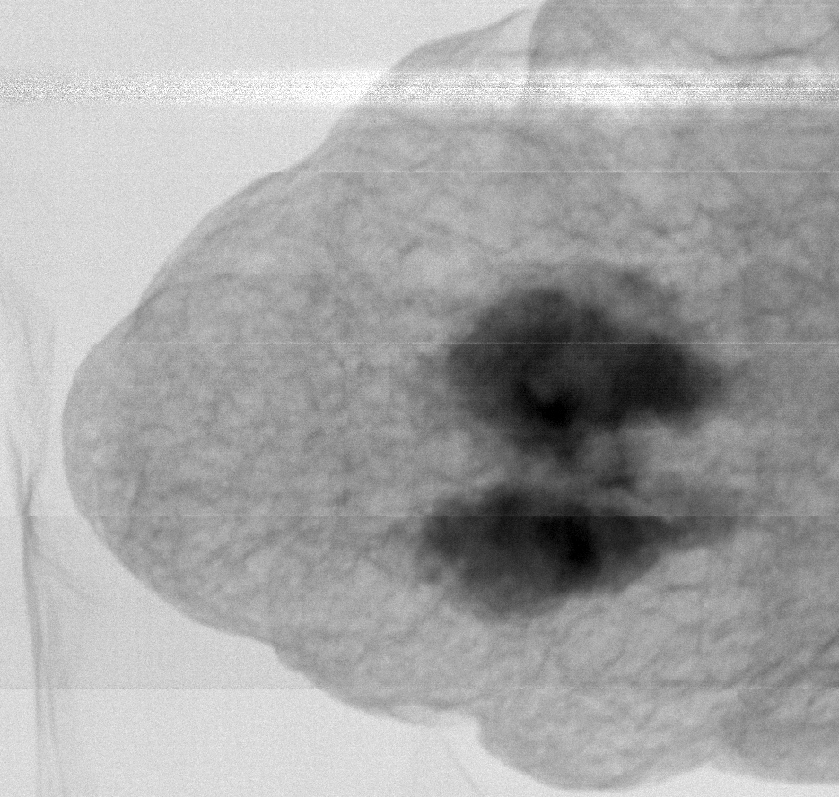
Tests were conducted using an industrial food screening machine. The main components of the machine are an X-ray tube, a belt feeder, and a linear scintillation X-ray detector. The detector was replaced by the presented camera (Fig. 11). Fig. 12 shows an image slice from scanning 30 m of croissants packed in cellophane bags. It shows both the chocolate filling and the packaging of the croissants. The recording length was chosen to confirm the camera continuous recording ability. (The camera memory can only store about 10 m of recording.) The enlarged image of the croissant (Fig. 13) confirms good image quality and the streak visible in the image is due to an imperfection in the bonding of one of the CdTe detectors with the chip.

In general, CdTe detectors are suitable for inspecting any object that can be overexposed to radiation with energies ranging from 25 keV to 100 keV.
Conclusions
This paper presents a camera for X-ray screening of objects in motion using an on-chip TDI. First, the limitation of the linear camera resolution is discussed. Then, an alternative approach of using a pixel array and the TDI method is presented. This is followed by a discussion of the TDI on-chip method that significantly improves the efficiency of the TDI method implementation. The following chapters are described in turn: the design of the detector module (which is an essential component of the camera), the architecture of the integrated circuit (which is an essential component of the detector module), and the architecture of the camera itself (both in terms of hardware and software). The last chapter presents the camera test performed on objects that are typically objects examined by this type of camera.
Acknowledgements
The work was created thanks to a project co-financed by the National Center for Research and Development under the “Path for Mazovia” program, contract: “MAZOWSZE/0099/19”.
The author would like to thank PID Polska Sp. z o. o. and, especially, Mr. Konrad Choręgiewicz for his help with the camera test measurements.
Also, the author would like to thank the Microelectronics group of the Department of Metrology and Electronics at AGH University of Krakow for their help with issues related to the detector module and, in particular, the integrated circuit.
References
-
Siewerdsen, J. H. et al. Empirical and theoretical investigation of the noise performance of indirect detection, active matrix flat-panel imagers (AMFPIs) for diagnostic radiology. Med. Phys. 24, 71–89 (1997). https://doi.org/10.1118/1.597919
-
Kraft, P. et al. Characterization and calibration of Pilatus detectors. IEEE Trans. Nucl. Sci. 56, 758–764 (2009).https://doi.org/10.1109/TNS.2008.2009448
-
Dinapoli, R. et al. A new family of pixel detectors for high frame rate X-ray applications. Nucl. Instrum. Methods Phys. Res. A: Accel. Spectrom. Detect. Assoc. Equip. 617, 384–386 (2010). https://doi.org/10.1016/j.nima.2009.10.043
-
Maj, P., Grybos, P., Kmon, P. & Szczygiel, R. 32k channel readout IC for single photon counting pixel detectors with 75 µm pitch, dead time of 85 ns, 9 e− rms offset spread and 2% rms gain spread. IEEE Trans. Nucl. Sci. 63, 1155–1161 (2016). https://doi.org/10.1109/TNS.2016.2523260
-
Ballabriga, R. et al. Review of hybrid pixel detector readout ASICs for spectroscopic X-ray imaging. J. Instrum. 11, P01007 (2016). https://doi.org/10.1088/1748-0221/11/01/P01007
-
Pangaud, P. et al. First Results of XPAD3, a New Photon Counting Chip for X-Ray CT-Scanner with Energy Discrimination. in IEEE Nuclear Science Symposium and Medical Imaging Conference NSS- MIC 14–18 (IEEE, 2007).
-
Bellazini, R. et al. Chromatic X-ray imaging with a fine pitch CdTe sensor coupled to a large area photon counting pixel ASIC. J. Instrum. 8, C02028 (2013). https://doi.org/10.1088/1748-0221/8/02/C02028
-
Ballabriga, R. et al. The Medipix3RX: a high resolution, zero-dead time pixel detector readout chip allowing spectroscopic imaging. J. Instrum. 8, C02016 (2013). https://doi.org/10.1088/1748-0221/8/02/C02016
-
Grybos, P. Front-end Electronics for Multichannel Semiconductor Detector Systems. (Oficyna Wydawnica Politechniki Warszawskiej, 2010).
-
McGregor, D. S. & Hermon, H. Room-temperature compound semiconductor radiation detectors. Nucl. Instrum. Methods Phys. Res. A: Accel. Spectrom. Detect. Assoc. Equip. 395, 101–124 (1997). https://doi.org/10.1016/S0168-9002(97)00620-7
-
Ovens, A. & Peacock, A. Compound semiconductor radiation detectors. Nucl. Instrum. Methods Phys. Res. A: Accel. Spectrom. Detect. Assoc. Equip. 531, 18–37 (2004). https://doi.org/10.1016/j.nima.2004.05.071
-
Locker, M. et al. Single photon counting X-Ray imaging with Si and CdTe single chip pixel detectors and multichip pixel modules. IEEE Trans. Nucl. Sci. 51, 1717–1723 (2004). https://doi.org/10.1109/TNS.2004.832610
-
Holdsworth, D. W., Gerson, R. K. & Fenster, A. A time-delay integration charge-coupled device camera for slot-scanned digital radiography. Med. Phys. 17, 876–886 (1990). https://doi.org/10.1118/1.596578
-
Zoladz, M., Grybos, P. & Szczygiel, R. X-ray imaging of moving objects using on-chip TDI and MDX methods with single photon counting CdTe hybrid pixel detector. J. Instrum. 16, C12014 (2021). https://doi.org/10.1088/1748-0221/16/12/C12014
-
Zoladz, M., Grybos, P. & Choręgiewicz, K. Test measurements of an ASIC for X-ray material discrimination by using on-chip time domain integration and a CdTe sensor. J. Instrum. 19, C03033 (2024). https://doi.org/10.1088/1748-0221/19/03/C03033