Iwona Rogalska1,2*
Marta Ruszałay1
Jakub Grendysa1,2
Anna Juś1
Renata Wojnarowska-Nowak1
Michał Marchewka1
Tomasz Wojtowicz2
Received 30 Aug. 2024
Received in revised form 29 Nov. 2024
Accepted 04 Dec. 2024
Available on-line 02 Feb. 2025
Keywords: HgCdTe; molecular beam epitaxy; infrared detectors.
A review of the specificity of the growth Hg1−𝑥Cd𝑥Te layers by molecular beam epitaxy (MBE) and results of experimental studies of several Hg1−𝑥Cd𝑥Te layers grown on Cd𝑦Zn1-𝑦Te (CZT) substrates are presented. It is well known that the performance of Hg1−𝑥Cd𝑥Te -based detectors strongly depends on the substrate material and its orientation. CZT substrates are among the most commonly used due to their very good lattice match with Hg1−𝑥Cd𝑥Te absorber material with different Cd content. In the present work, the authors focused on optimizing the MBE growth parameters in order to obtain the best possible crystalline quality of Hg1−𝑥Cd𝑥Te layers grown on CZT substrates with (211)B orientation, in particular in terms of minimizing the number of defects. Experimental results of the selected structures showed that the obtained undoped Hg1−𝑥Cd𝑥Te layers of different x have high crystallographic and optical quality, as well as good surface morphology. In particular, high-resolution X-ray diffraction (HRXRD) measurements and their analysis showed that the best structure has a full width at half maximum of rocking curve (FWHM𝑅𝐶) as low as 21.5 arcsec, and that the intensity distribution of diffraction peaks does not indicate the influence of mosaicisity and dislocation density.
HgCdTe is a ternary alloy semiconductor that crystallizes in a zinc blende structure. Mixing alloys of two zinc blende compounds: HgTe and CdTe can cover all important infrared (IR) ranges, that is from 1 μm to 30 μm, by changing the ratio of Cd and Hg [1–3]. Furthermore, the lattice constant of Hg1−𝑥Cd𝑥Te changes by only 0.3% throughout the composition range, that is, from x = 0 to 1. The primary substrate used to grow HgCdTe is semi-insulating (211)B CD0.96Zn0.04Te, with lattice matched. To align the lattice with Hg0.7Cd0.3Te, 4% ZnTe is added to CdTe, facilitating epitaxial growth without misfit dislocations. The IR transparency of the CdZnTe substrate makes it ideal for growing HgCdTe materials used in applications in a wide range of IR. When grown on (211)B substrates, HgCdTe typically exhibits a smooth, defect-free surface morphology. However, it requires a higher mercury flux compared to (111)B substrates to achieve stoichiometric growth [3–5]. Previous substrates such as CdTe (111) and (100) resulted in epilayers with high densities of twins and hillocks [5]. The (211)B orientation has a higher step density than the (111) orientation, making it more resistant to dislocations and twinning faults [3, 5]. One major drawback of growing in the orientation (211) B is the narrow temperature window required for high-quality HgCdTe growth, which requires precise control of substrate temperature to within ± 5 °C.
The growths are performed in a Riber Compact 21 molecular beam epitaxy (MBE) system equipped with a liquid Hg source and a reflection high-energy electron diffraction (RHEED) system. HgCdTe growth is most commonly performed using a binary source of CdTe, and elemental Hg and Te. Basically, Hg evaporates and Cd sublimates as single monomers, while Te sublimates as a Te2 dimer.
Using CdTe instead of elemental Cd provides better control over the alloy composition. CdTe sublimates congruently as Cd and Te2 species, while HgTe evaporates incongruently due to the weak Hg–Te bond. This allows for precise control over the growth rate and x-composition of the Hg1−𝑥Cd𝑥Te epilayers. First, the Hg/Te flux ratios must be optimized and in the authors’ case they were in the range of 185–200. In this work, HgCdTe material epilayers were grown on 1 cm × 1 cm CD0.96Zn0.04Te (211)B substrates. Before being loaded into the MBE system, each substrate must undergo chemical cleaning to eliminate dust and residual contamination, followed by etching to remove polishing damage. Chemical etching is performed with a 0.12% bromine methanol solution for 7 s to expose a fresh CdZnTe surface. The etched wafer is dried in a stream of ultrapure N2 gas and then attached to the molybdenum (Mo) holder using Ga–In eutectic. The surface quality of the substrate is crucial for achieving high-quality HgCdTe epilayers in subsequent growth. The goal of the present work was to optimize the growth processes aiming to obtain high-quality HgCdTe layers with an acceptable dislocation density [6, 7].
First, the Mo holder with the substrate is transferred from the loading chamber to the preparation chamber, where it is heated under vacuum conditions for several minutes to remove any H2O present on the surface. Next, the holder is moved to the growth chamber via the analysis chamber, where the temperature is raised to 300 °C and maintained for 10 to 15 min. This high temperature thermally cleans the substrate of any native oxides and excess Te, which is always present on CdZnTe substrates after Br/methanol etching, as Br preferentially etches Cd, leaving a Te-rich surface. The thermal cleaning process is periodically monitored using the RHEED screen. Initially, spots on the screen indicate the presence of excess Te on the substrate surface. As thermal cleaning progresses, a sharp streaky pattern develops and the spots gradually disappear, leaving long, light streaks. The substrate temperature is then reduced to the optimal growth temperature (175–185 °C in the authors’ case) and stabilized, along with the cell temperatures. Growth nucleation begins when the shutters are opened. During nucleation, the RHEED pattern of the growing crystal is closely monitored to optimize growth parameters. Mercurydeficient growth during nucleation is indicated by spots on the RHEED screen. The mercury flux can be adjusted by controlling the cell temperature, and any mercury deficiency can be compensated by increasing the mercury flux or lowering the substrate temperature. HgCdTe growth is maintained under optimal conditions through frequent in situ observations of RHEED patterns and real-time monitoring of substrate and cell temperatures. The desired x-value of HgCdTe epilayers is achieved by selecting an appropriate growth temperature and optimizing a beam equivalent pressure (BEP) of the molecular beams. The BEP for all materials is determined by measuring the difference between the beam pressure when the cell shutter is open and the background pressure when the shutter is closed.
This measurement is taken before heating the mercury cell or starting any growth, as high mercury pressure in the chamber makes background flux measurements inaccurate once the mercury cell is operational. After reaching the desired epilayer thickness, all shutters are closed except for the Hg shutter. The structure is then gradually cooled to approximately 80 °C under mercury flux to prevent mercury desorption from the surface of the epilayer at elevated temperatures, thus avoiding the formation of mercury vacancies. Alternatively, a thin Hg1−𝑥Cd𝑥Te capping/passivating layer with a high x value can be grown on the surface of the HgCdTe epilayer to prevent Hg desorption. The precise control of growth temperature is crucial for the crystal quality of HgCdTe epitaxial films. Therefore, the substrate temperature is meticulously regulated by a proportional integral derivative (PID) feedback using a Ga-wetted thermocouple in direct contact with the sample holder. The thermocouple was carefully calibrated at the melting points of indium and tin. The quality of the obtained epilayers was evaluated using a number of post-growth characterization techniques. These techniques included high-resolution X-ray diffractometry (HRXRD), Fourier transform infrared (FTIR) spectroscopy, and both optical and confocal microscopy.
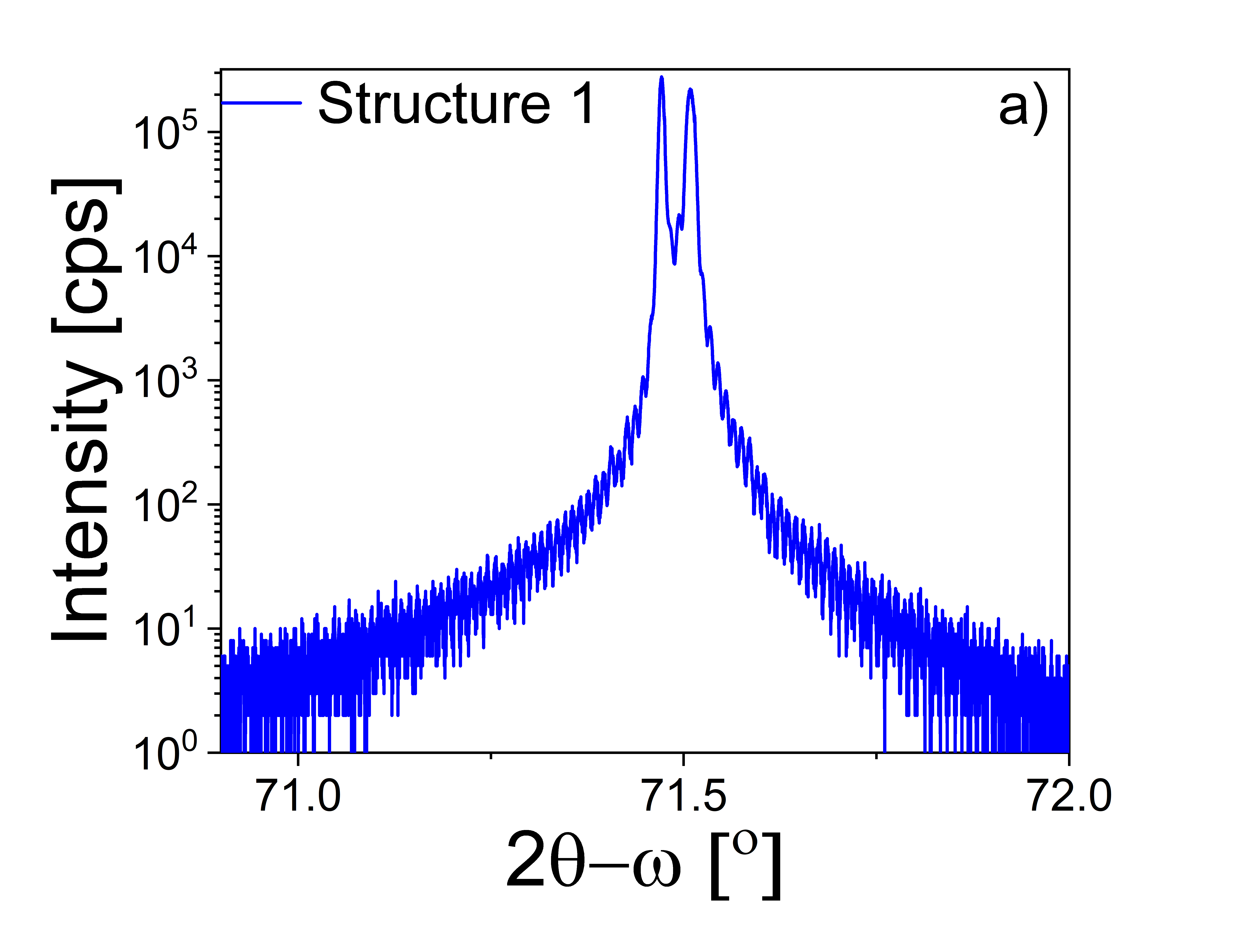
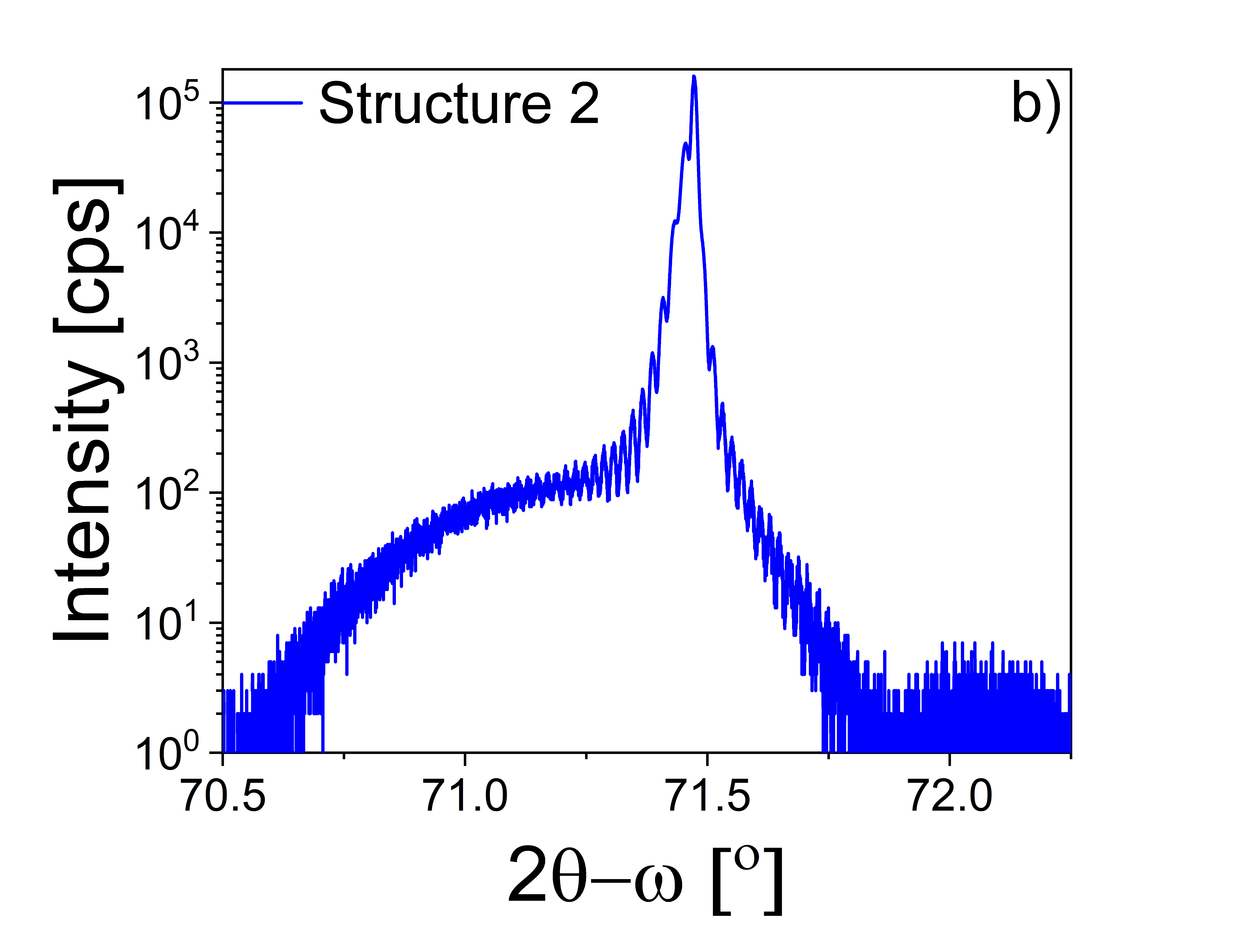
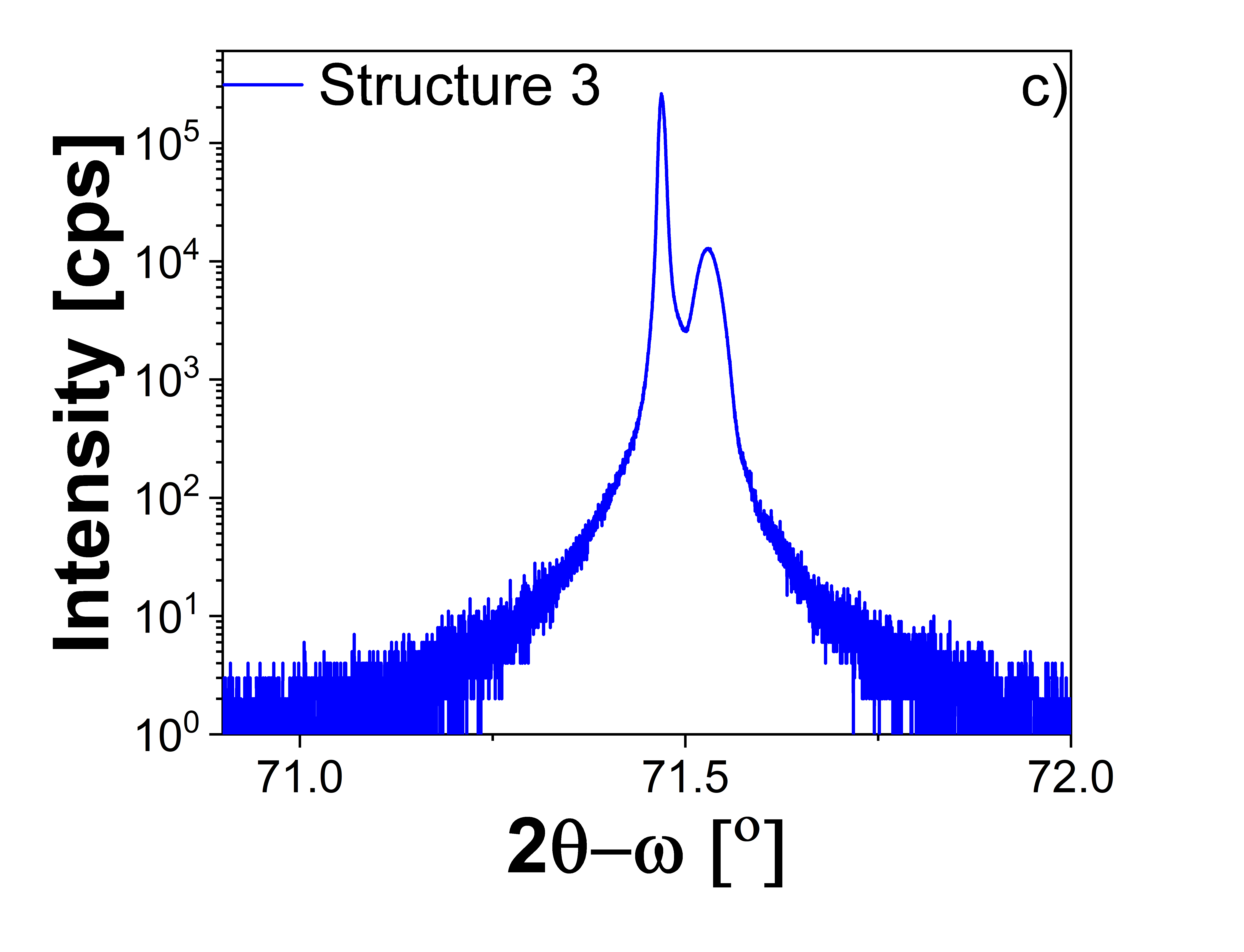
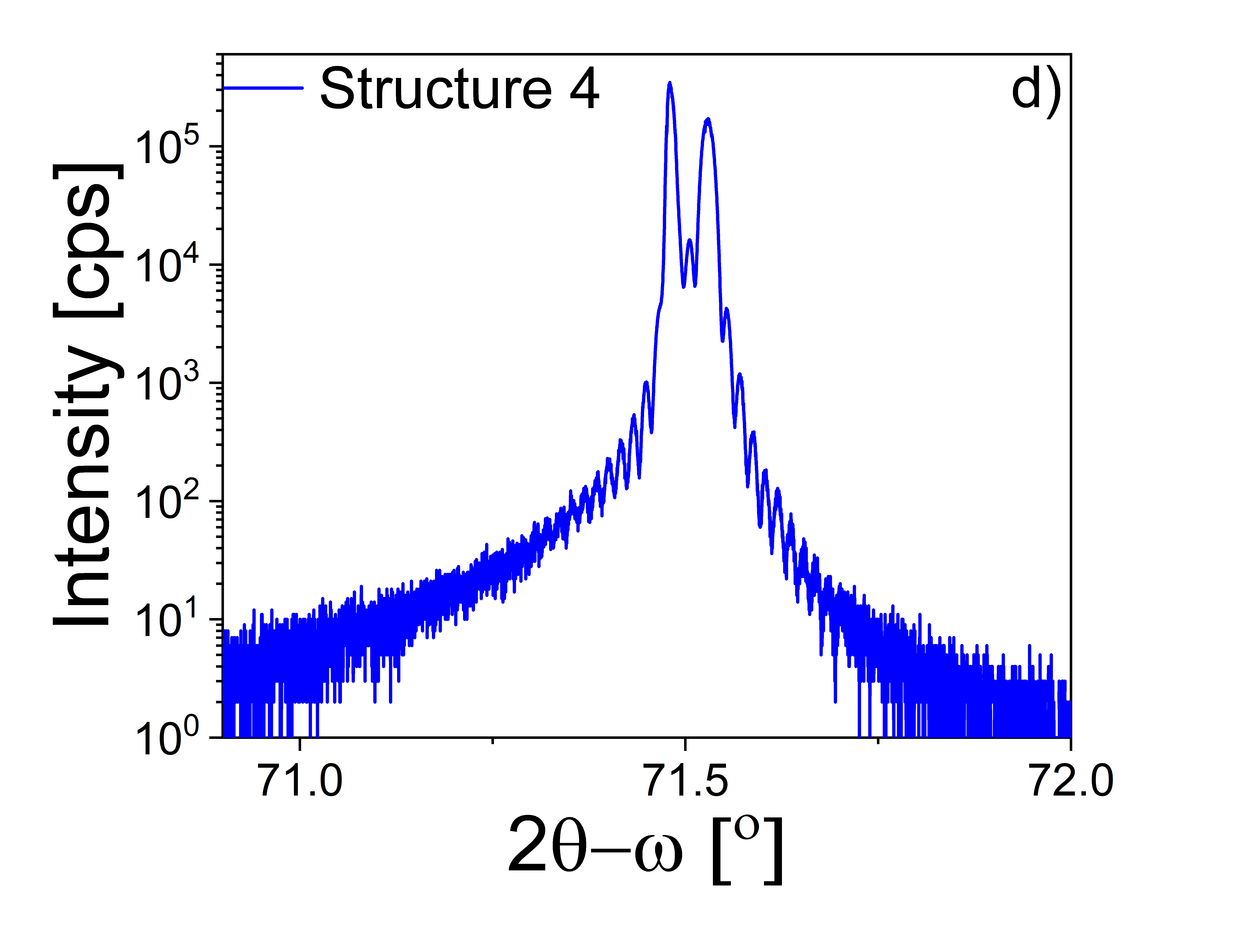
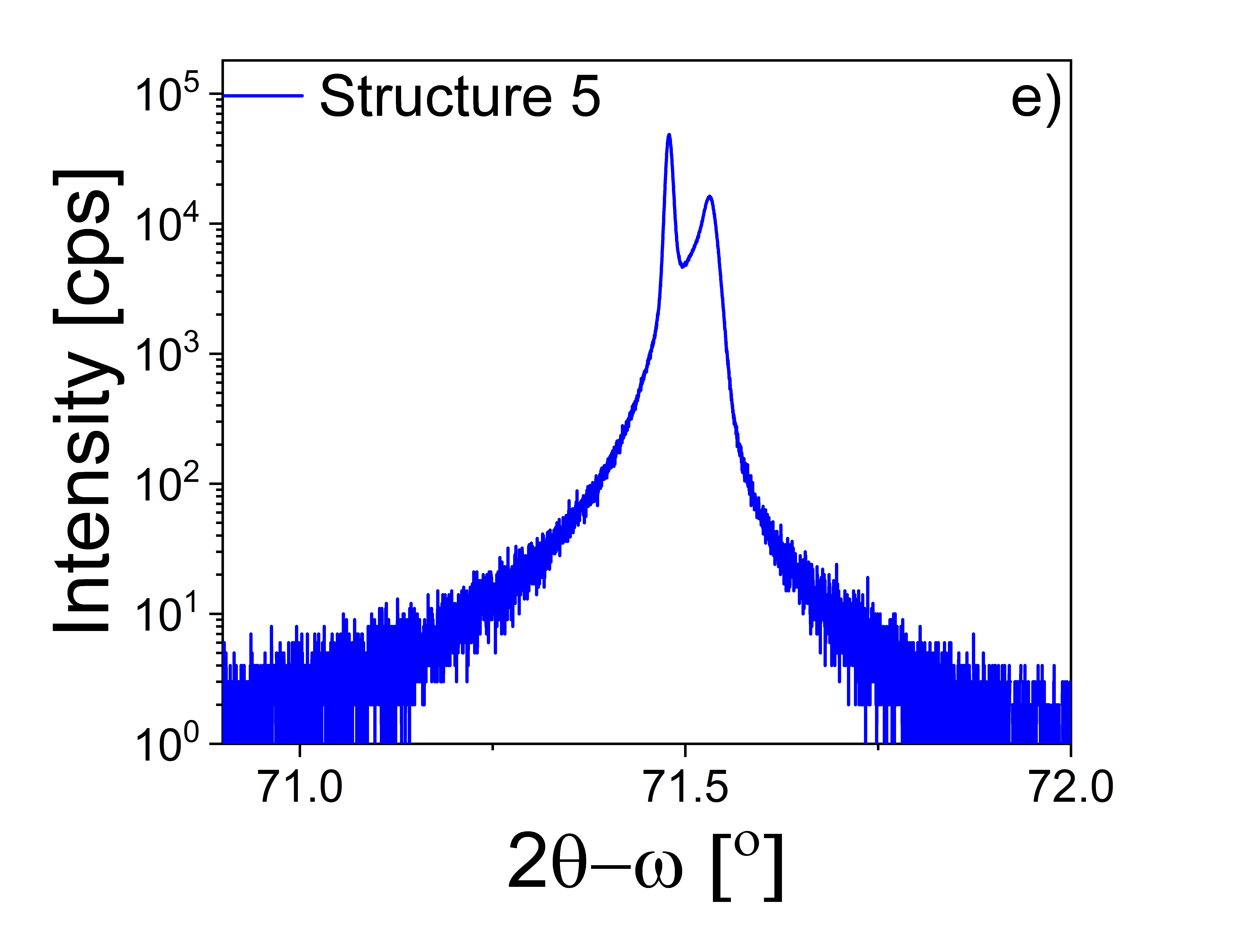
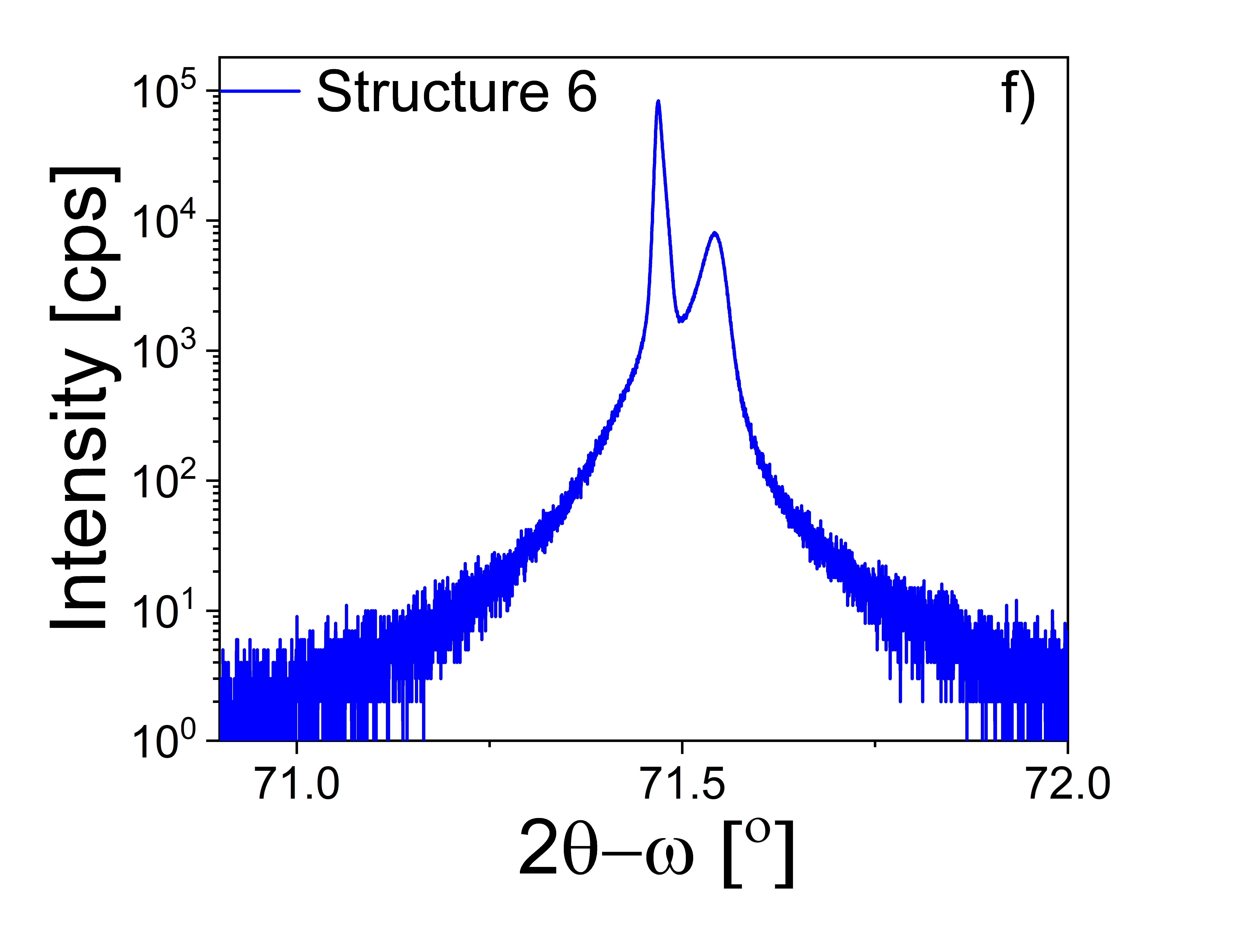
The crystal quality of the grown HgCdTe films is evaluated using 2Θ − 𝜔 scans and the full-width at half maximum (FWHM) of the X-ray double-crystal rocking curve (DCRC). For this purpose, all six structures discussed here were examined by HRXRD - see Fig. 1. The same measurement parameters were kept for all samples, that is the step size and counting time equal to 0.0002◦/s and 0.3 s for 2Θ − 𝜔 scans and 0.0002◦/s and 0.1 s for 𝜔-RC scans, respectively.
The scans were performed in the triple-axis configuration, adjusting to the substrate in a symmetrical scan 422. In each diffractogram, two distinct diffraction peaks are apparent. For all structures studied, the peaks originating from the CdZnTe substrate exhibit the highest intensity, while those from the CdHgTe layer display a lower intensity. For peaks from both the substrate and mercury cadmium telluride (MCT) layer, the lattice constant and FWHM were determined. Using Panalytical ’Amass’ program, numerical simulations were conducted to ascertain the composition and thicknesses of the layers. The values are given in Table 1 and Table 2.
Table 1.
XRD results for epitaxially grown Hg1−𝑥Cd𝑥Te on Zn1−𝑦Cd𝑦Te (211)B substrates.
Structure name |
Material |
2Θ(◦) |
2Θ − 𝜔 FWHM (arcsec) |
Alloy comp. x, y |
Structure 1 (E016Z23) |
Zn1−𝑦Cd𝑦Te - Hg1−xCdxTe |
71.4714 71.5089 |
25.7 39.7 |
0.96 0.26 |
Structure 2 (E013Z23) |
Zn1−𝑦Cd𝑦Te - Hg1−xCdxTe |
71.4731 71.4543 |
39.3 76.9 |
0.96 0.37 |
Structure 3 (E092Z23) |
Zn1−𝑦Cd𝑦Te - Hg1−xCdxTe |
71.4694 71.5284 |
29.5 122.8 |
0.96 0.21 |
Structure 4 (E085Z23) |
Zn1−𝑦Cd𝑦Te - Hg1−xCdxTe |
71.4808 71.5289 |
34.7 57.2 |
0.96 0.24 |
Structure 5 (E074Z23) |
Zn1−𝑦Cd𝑦Te - Hg1−xCdxTe |
71.4789 71.5312 |
32.4 69.9 |
0.96 0.23 |
Structure 6 (E061Z23) |
Zn1−𝑦Cd𝑦Te - Hg1−xCdxTe |
71.4694 71.5392 |
37.2 120.5 |
0.96 0.22 |
Table 2.
Quantitative comparison of Hg1−𝑥Cd𝑥Te epitaxially grown on CdZnTe (211)B substrates.
Structure name |
𝑇𝑠𝑢𝑏 (°C) |
Factor Cd/Te |
Factor Hg/Te |
Epilayer x – value XRD |
Epilayer x – value FTIR |
𝐸𝑔 – value FTIR (eV) |
Rocking curve FWHM (arcsec) |
Thickness of epilayer XRD (μm) |
Thickness of epilayer SEM (μm) |
Dislocation density (cm-2)×105 |
Mosaicity (×10-6) |
Structure 1 (E016Z23) |
185 |
0.071 |
187 |
0.26 |
0.25 |
0.237 |
21.5 |
1.07 |
1.08 |
1.35 |
– |
Structure 2 (E013Z23) |
185 |
0.079 |
151 |
0.37 |
0.31 |
0.307 |
27.1 |
0.53 |
0.6 |
1.97 |
– |
Structure 3 (E092Z23) |
175 |
0.057 |
185 |
0.21 |
0.21 |
0.186 |
57.8 |
– |
0.82 |
3.58 |
0.56 |
Structure 4 (E085Z23) |
180 |
0.055 |
187 |
0.24 |
0.23 |
0.200 |
58.2 |
0.66 |
0.67 |
1.99 |
0.41 |
Structure 5 (E074Z23) |
185 |
0.043 |
172 |
0.23 |
0.21 |
0.184 |
309.2 |
– |
2.5 |
2.96 |
134.84 |
Structure 6 (E061Z23) |
185 |
0.056 |
200 |
0.195 |
0.20 |
0.164 |
327.0 |
– |
1.6 |
3.89 |
4.88 |
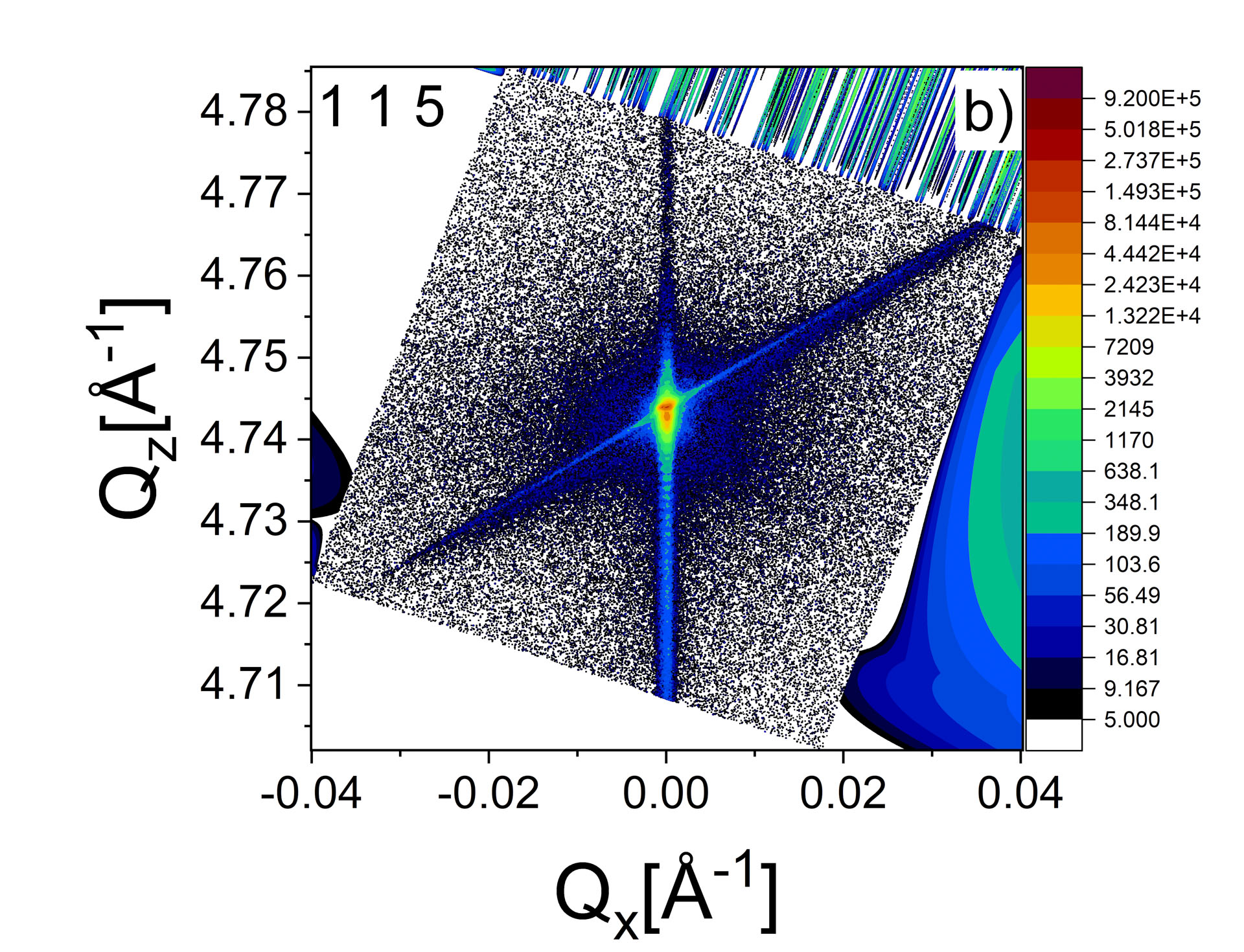
Fig. 1 illustrates the 2Θ−𝜔 XRD scan for all the studied structures. The visible peak from the CdZnTe substrate was recorded at a position of about 71.5°. Peaks from the HgCdTe layers were also observed nearby. The measured range of the FWHM2Θ−𝜔 of the HgCdTe is between 39 and 123 arcsec and the Cd contents determined from the simulation of the HRXRD measurements for investigated structures are presented in Table 1. Based on the thickness fringes seen for Structures 1, 2, and Structure 4, layer thicknesswas determined using Amass software and summarised in Table 2. The authors have analysed the strain relaxation of thin HgCdTe structures using a 2-dimensional (2D) reciprocal space mapping of XRD. This technique has recently become a powerful tool for strain and structural characterization of epilayers and heterostructures [8–12]. Triple-axis diffractometry, being non-destructive, provides highly precise measurements of strain and dislocation densities over large sample areas. Recent advancements have enabled this method to extract detailed information on defects, dislocation densities in strain-relaxed heterostructures, and the static distribution of microdefects by analysing the diffuse scattering around coherent Bragg reflection peaks in reciprocal space [6]. Furthermore, the scope of X-ray measurements was expanded to encompass a reciprocal space map (RSM). These mapping procedures were conducted using symmetric reflection 422 and asymmetric reflection 115 (see Fig. 2 and Fig. 3). RSM data were carried out in coplanar geometry, conducting a 2Θ − 𝜔 relative scan. Each step in the scan had time per step equal to 10 s, with a step size of 0.0008 for 𝜔 and 0.01 for 2Θ. RSM coordinates are displayed in Å−1 units for both Qx and Qzcoordinates.
The asymmetric (115) maps show that all the MCT layers are perfectly aligned with the substrate, which means that they are almost completely strained against it. By analysing the shapes of the reciprocal space points, structural features such as mosaics and diffuse scattering can be observed [6-13,15]. RSM obtained for Structures 1 and 2 show features of diffusive scattering. RSM obtained for Structure 2 [Fig. 2(b)] confirmed its outstanding crystal quality. Based on the angular positions of the reciprocal space points, a lattice mismatch was calculated, which was 225 ppm, –453 ppm, –886 ppm, –635 ppm, –594 ppm, and –726 ppm for Structures 1–6. This indicates the presence of compressive strain in Structure 2 and tensile strain in others [16]. The reciprocal lattice points coming from both the substrate and the layer for the Structure 2 are quite narrow in both the Qx and Qzdirections. They lie in the range of –0.02 Å−1 ≤ Qx ≥ 0.02 Å−1 and –0.02 Å−1 ≤ Qz ≥ 0.02 Å−1. Minimal diffuse scattering is apparent, confirming the good quality of this structure. Furthermore, a crystal truncation rod (CTR) is visible, as well as fringes. This falls within the range of –0.02 Å−1 ≤ Qx ≥ 0.02 Å−1 and –0.015 Å−1 ≤ Qz ≥ 0.015 Å−1. The largest diffusion scattering occurs for Structure 5. It is in the range of –0.032 Å−1 ≤ Qx ≥ 0.032 Å−1 and –0.015 Å−1 ≤ Qz ≥ 0.015 Å−1 as can be seen in Fig. 2(e) [17].
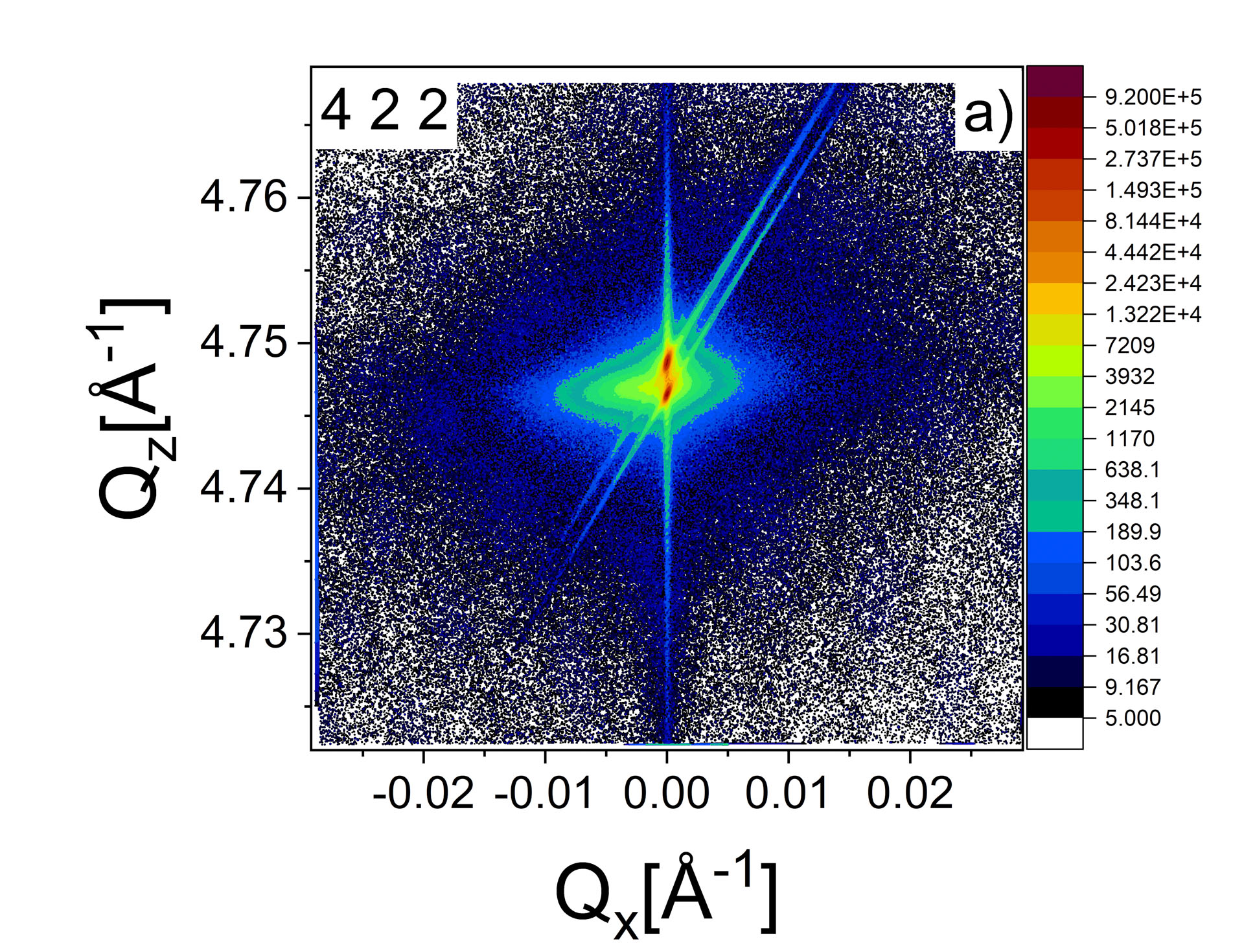
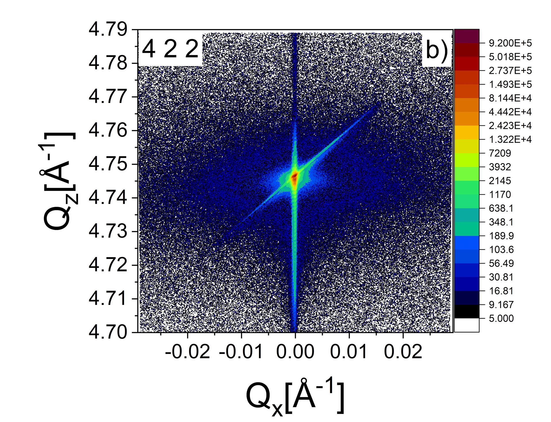
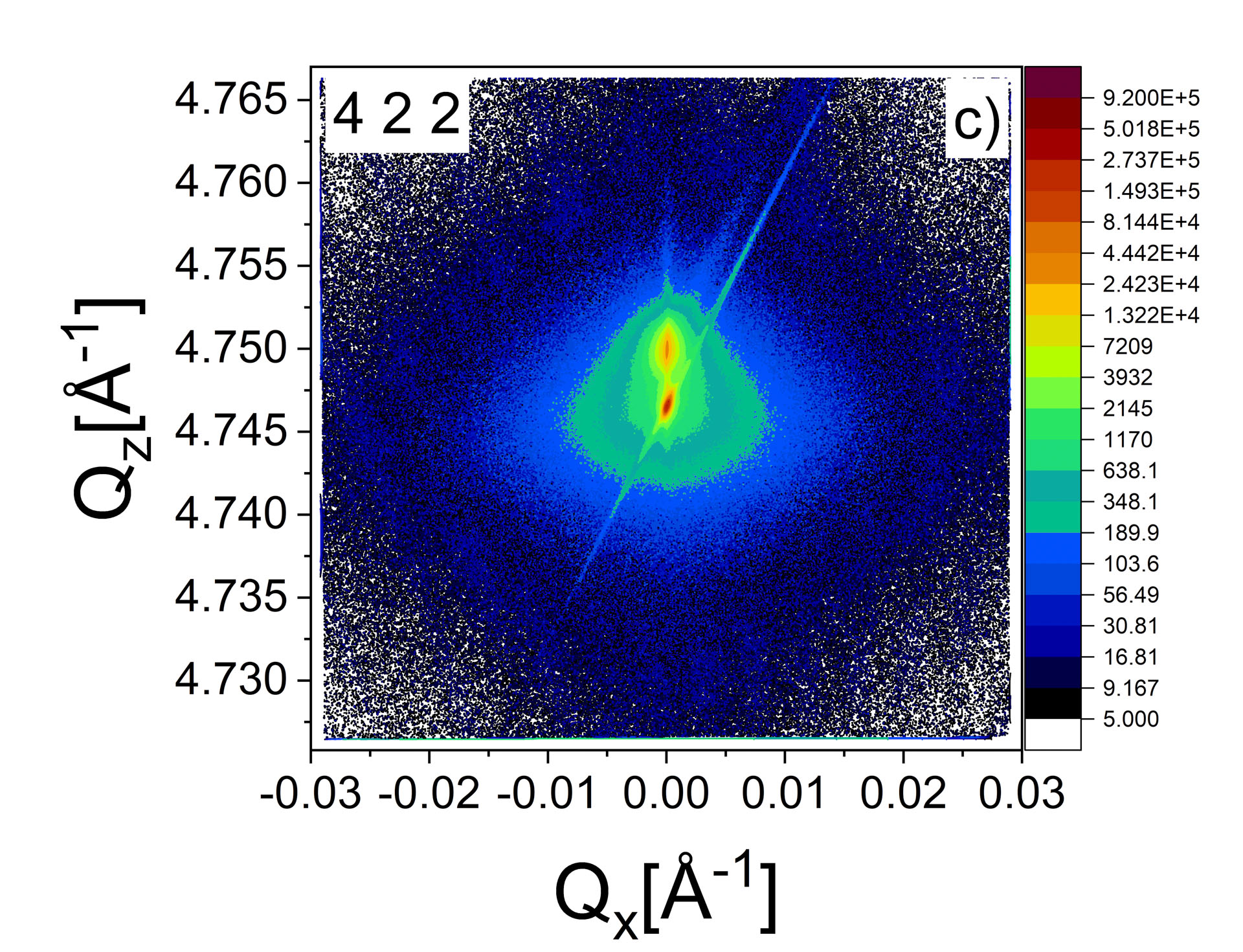
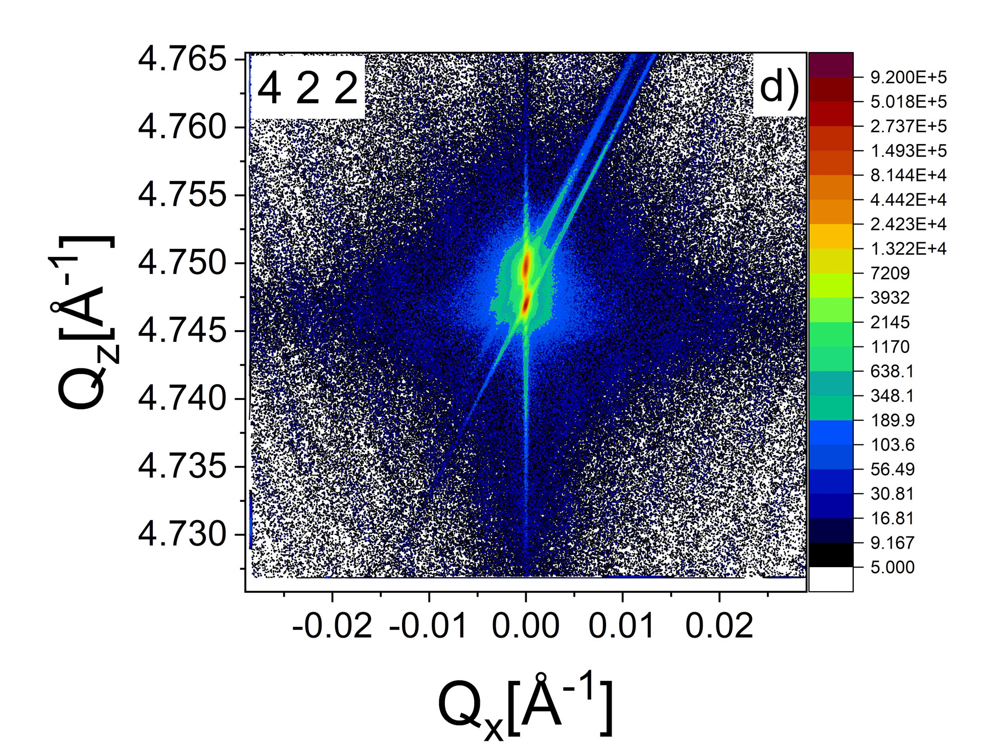
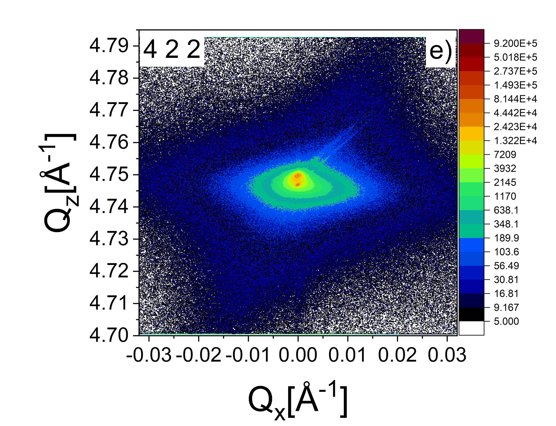
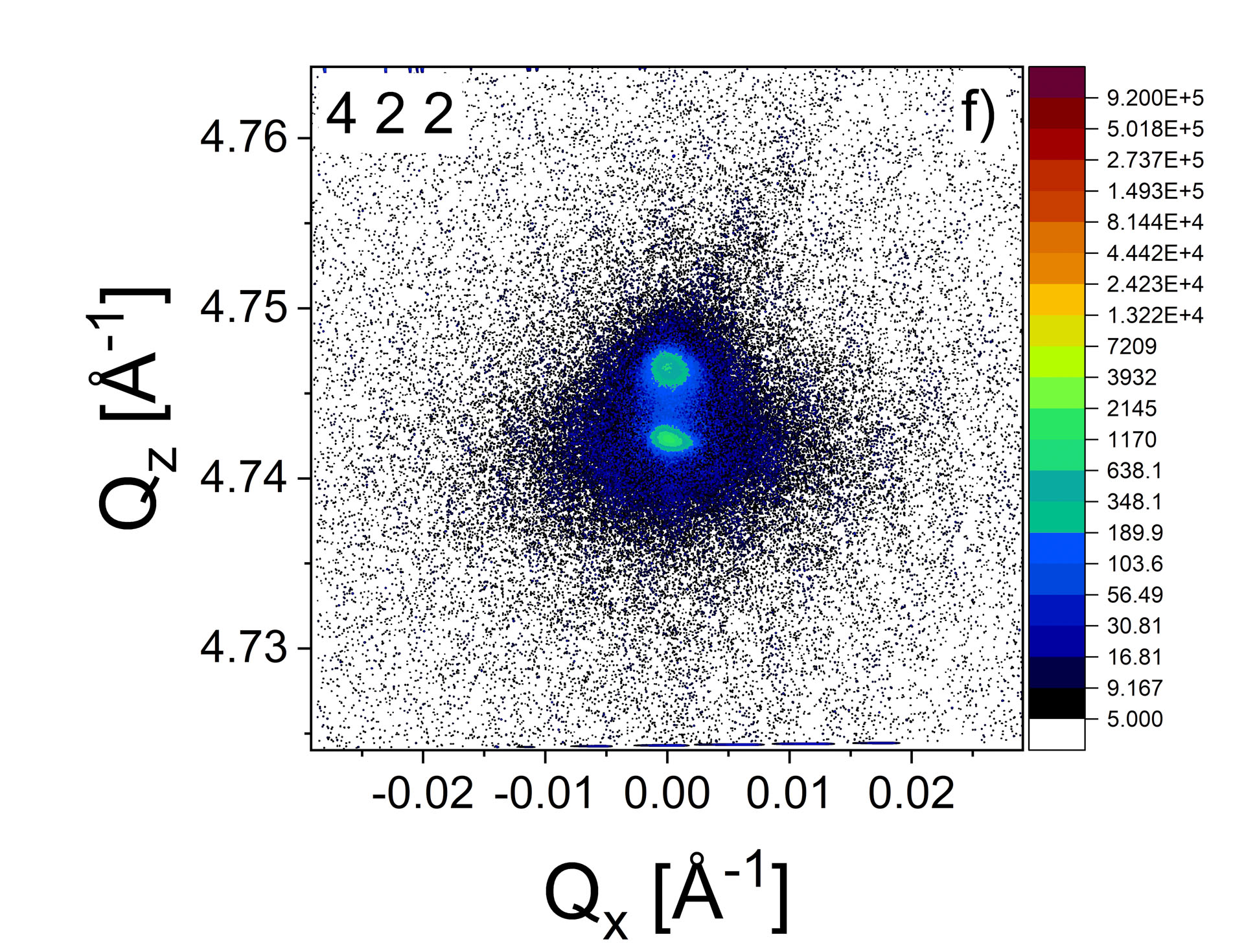
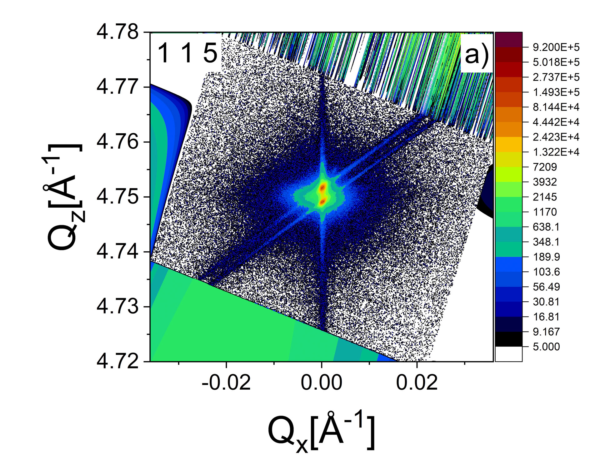
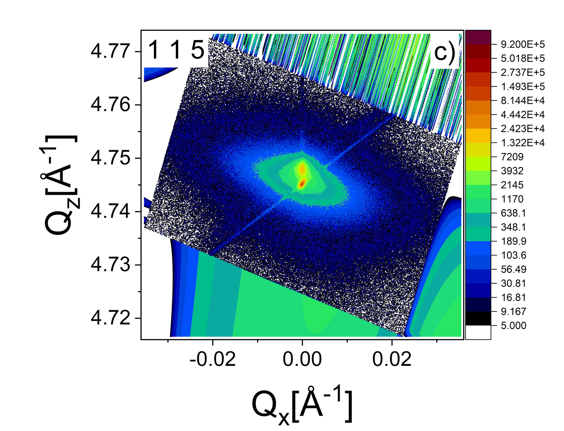
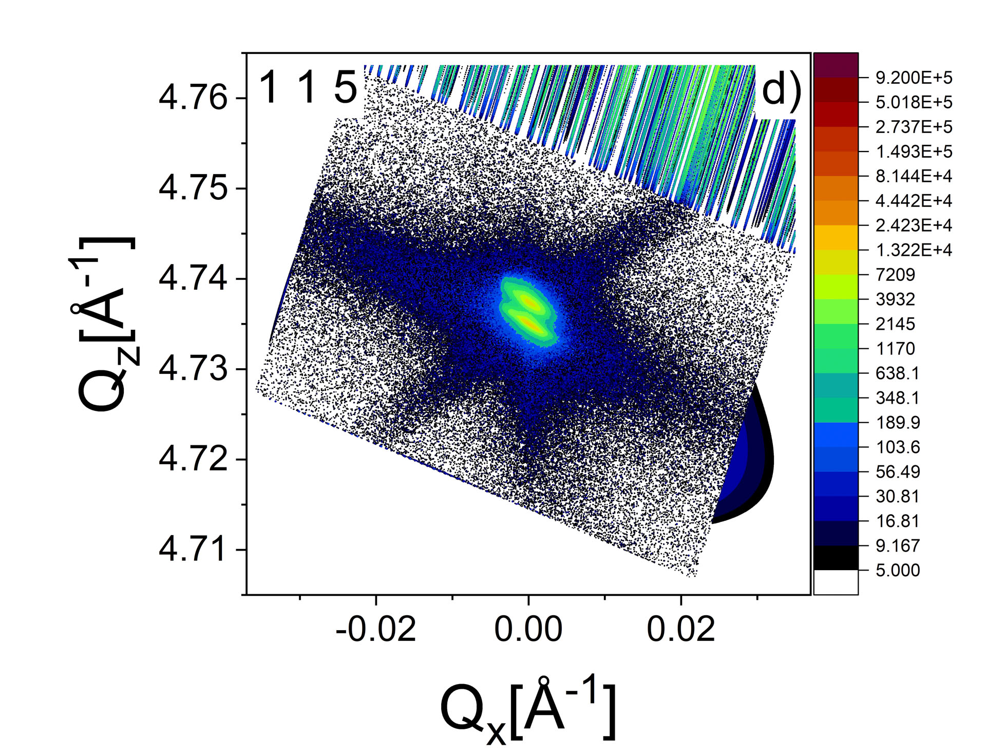
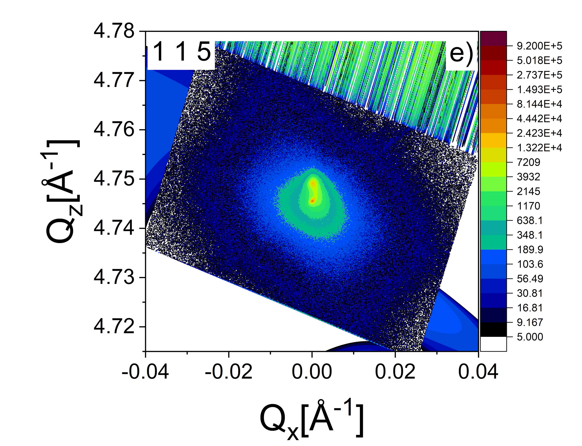
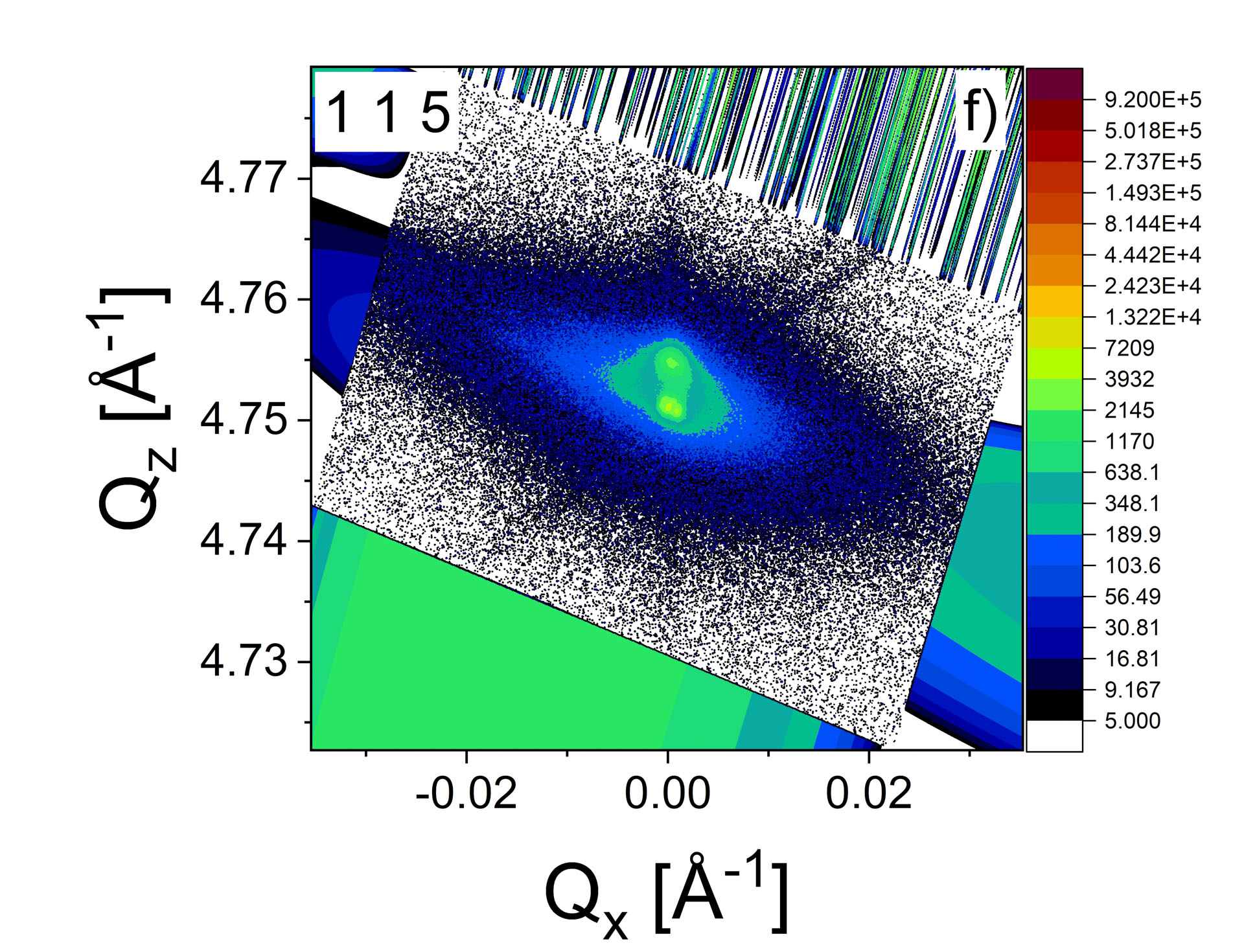
This contrasts significantly with Structures 5, 4, and 3, where observable features include diffuse scattering and mosaic characteristics. Unlike the previously discussed structures, in this case there are no visible CTRs or fringes. The diffuse scattering is prominent in both directions and diminishes within the ranges of –0.001 Å−1 ≤ Qx ≥0.013 Å−1 and –0.009 Å−1 ≤ Qz ≥ 0.006 Å−1 for Structure 5, –0.003 Å−1 ≤ Qx ≥ 0.003 Å−1 and –0.002 Å−1 ≤ Qz ≥ 0.002 Å−1 for Structure 4 and for Structure 3 –0.005 Å−1 ≤ Qx ≥ 0.006 Å−1 and –0.002 Å−1 ≤ Qz ≥ 0.004 Å−1. Mosaicitywas computed on the basis of methodology described in [6, 13] , and the values are given in Table 2.
The results indicate that the HgCdTe films exhibit good crystalline quality, with no significant dislocation proliferation in the HgCdTe epitaxial layer compared to the substrate.
MBE-grown structures are inspected using optical microscopy immediately after unloading from the MBE system. The Nomarski contrast imaging mode is employed due to its high resolution and clarity compared to other imaging modes for thin-film structures [18]. The surface macrodefects of HgCdTe films can be categorized into two types: those related to suboptimal growth conditions, such as growth temperature and flux ratio, and those related to the surface condition of the polished Cd𝑦Zn1-𝑦Te (CZT) substrate. Macrodefects arising from growth conditions can be effectively eliminated by precisely controlling the growth temperature and adjusting the Hg/Te flux ratio. Consequently, the remaining surface macrodefects primarily originate from surface imperfections in the CZT(211)B substrate after polishing or corrosion.
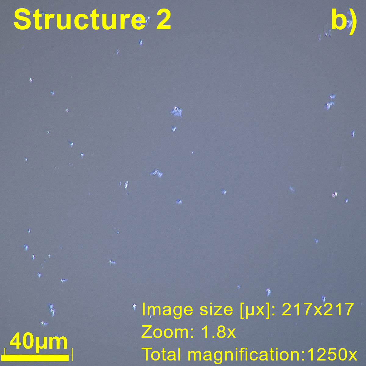
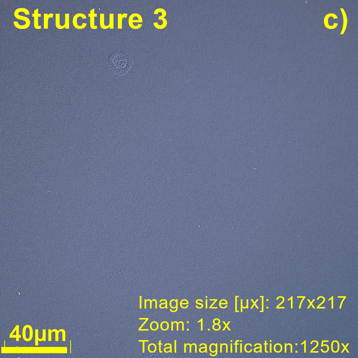
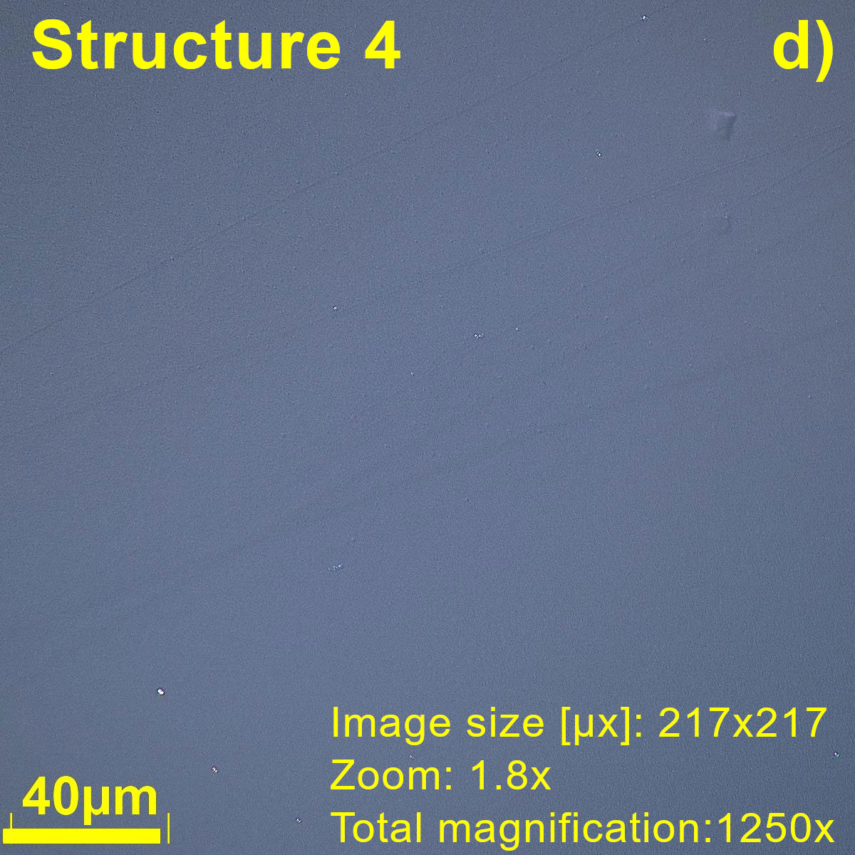
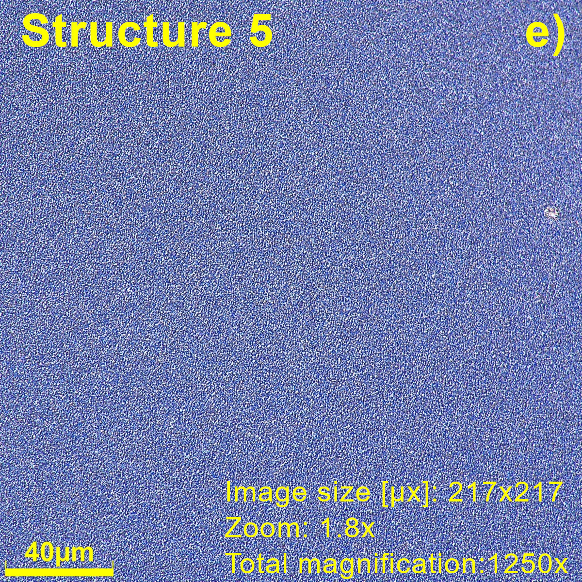
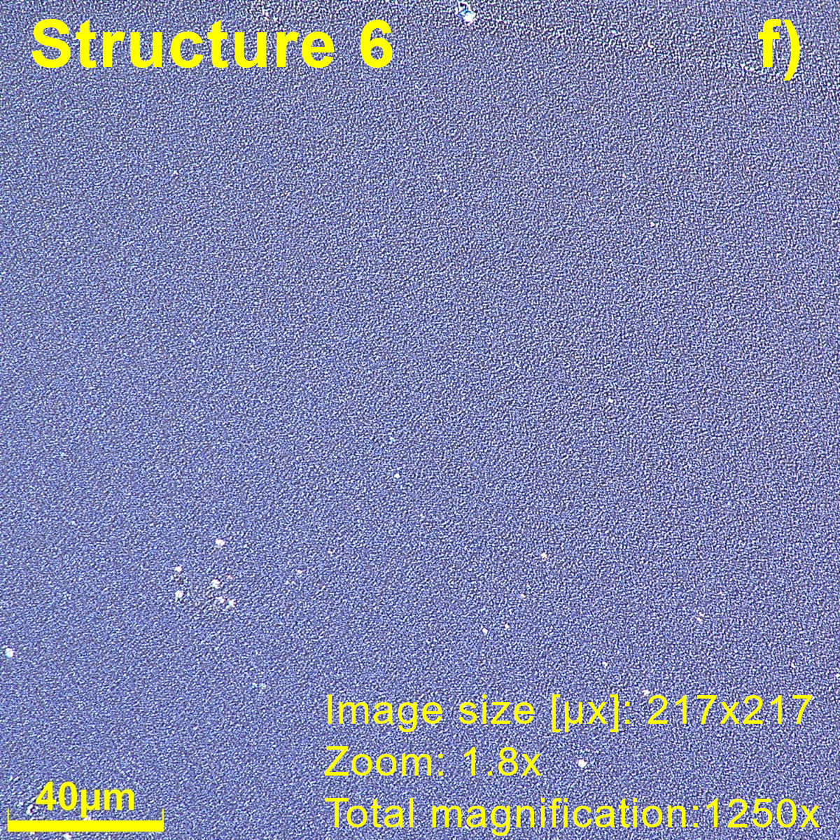
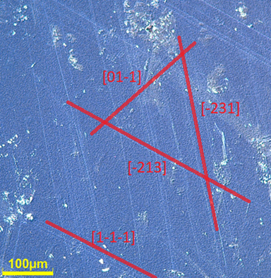
Nomarski microscopy, using interferometry, allows the observation of subtle changes in the height or refractive index of the structure, providing high resolution and contrast compared to other imaging techniques, used for thin-film characterization [19]. Images of the layers surface show defects that change in individual structures. In the case of Structure 2, there are visible defects on the surface, but its root mean square (RMS) roughness in clean areas is equal to 16.45 nm [Fig. 4(b)]. Structures 5 and 6 have higher roughness, but are free of significant surface defects visible by optical microscopy. On the other hand, Structures 4 and 3 have low roughness, in addition, there are lines visible on the surface of Structure 4 [Fig. 4(d)] in the image at approximately ×1250 and Structure 6 [Fig. 4(f)]. Crosshatched patterns, consisting of crossed lines at 44- to 45-degree angles, are typically found on the surfaces of MBE-grown HgCdTe epilayers of relatively high quality, with low densities of micro or macrodefects on (211)B CdZnTe bulk substrates [20]. Fig. 5 shows the characteristic crosshatched pattern of HgCdTe grown by MBE on a (211)B CdZnTe substrate for Structure 6. The hatch pattern on the surface of (211) B includes three sets of lines parallel to the [232], [213], [011], and [130] directions. The lines on Structure 4 are much more subtle.
Optical transmission experiments were used to determine the HgCdTe layers composition. This involved measuring spectra across a wide wavelength range on both sides of the absorption bandgap edge, utilizing a FTIR spectrometer. For this purpose the Vertex 80 Bruker FTIR spectrometer was used. Due to the high transparency of the CdZnTe substrate up to a wavelength of 30 μm, most IR radiation reaches the HgCdTe epilayer in backside illuminated structures, although some losses occur due to reflection at the substrate interface [6]. The measurements were made in the medium infrared range (500–8000 cm-1), in transmission mode, at room temperature. It is clearly visible in Fig. 6, that the optical properties (transmittance level) change depending on the wavelength. The absorption coefficient was determined from transmission spectra using the equation: 𝛼=-1𝑑 ln(T), where 𝛼 is the absorption coefficient, d is the thickness of the thin film, T is the transmission. The thickness of the HgCdTe films was determined by a side-view scanning electron microscopy (SEM) and the values are given in Table 2. The magnitude of absorption coefficient is high and for all six studied structures, it is of the order of 104 cm-1. The results of optical measurements were used to determine the E𝑔 for each sample. It is known that the absorption coefficient increases sharply with photon energy beyond the fundamental absorption edge. To obtain the electronic bandgap of samples, the square of the absorption coefficient was calculated. The 𝛼2 of all six studied structures as a function of energy is shown in Fig. 6. The linear fit of curve allows to obtain the value of E𝑔, which are presented in Table 2. The lowest values were recorded for Structure 6 (E𝑔 = 0.164 eV), Structure 5 (E𝑔 = 184 eV), Structure 3 (E𝑔 = 0.186 eV), Structure 4 (E𝑔 = 0.2 eV). The highest values were noted for Structure 1 (E𝑔 = 0.237 eV) and Structure 2 (E𝑔 = 0.307 eV).
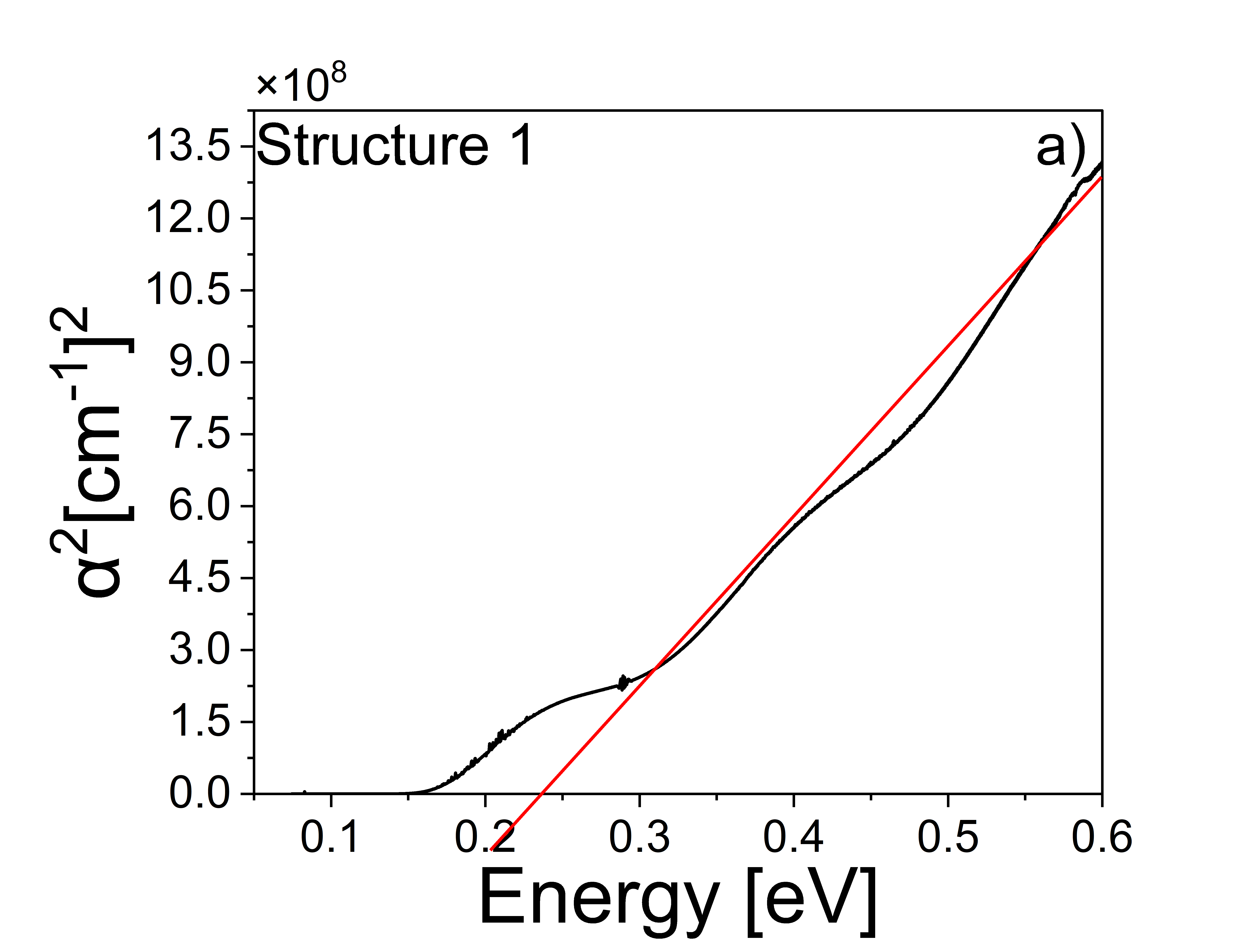
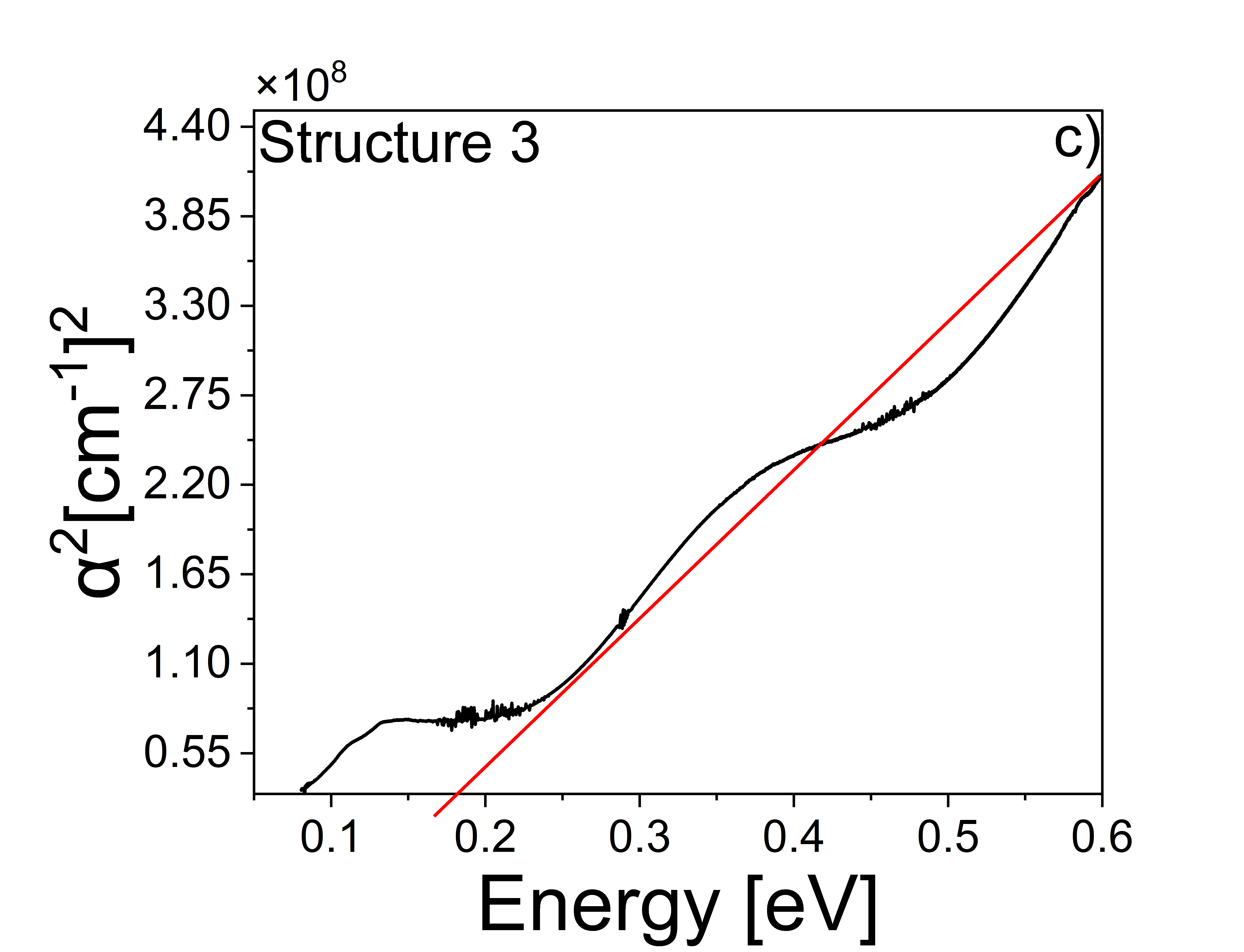
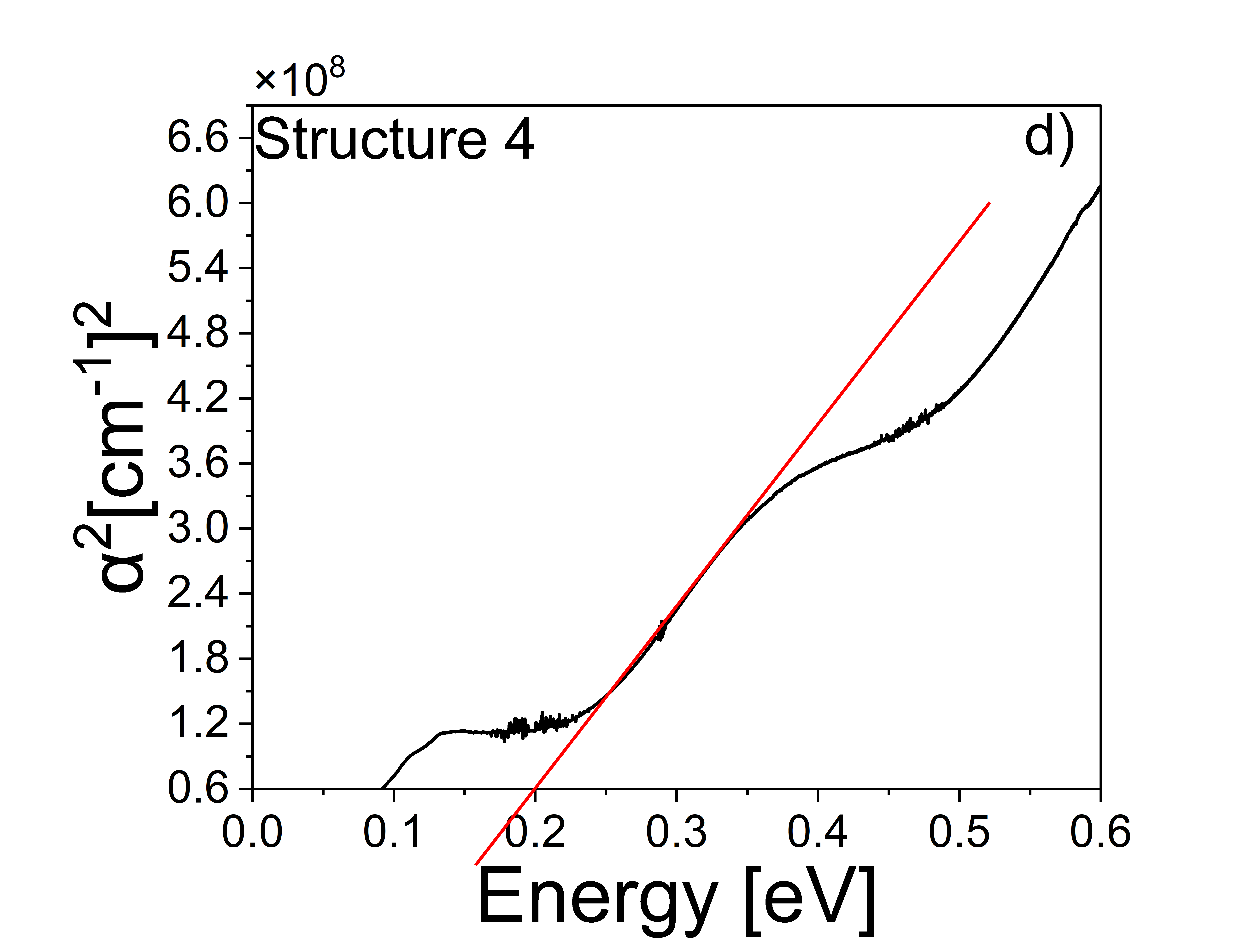
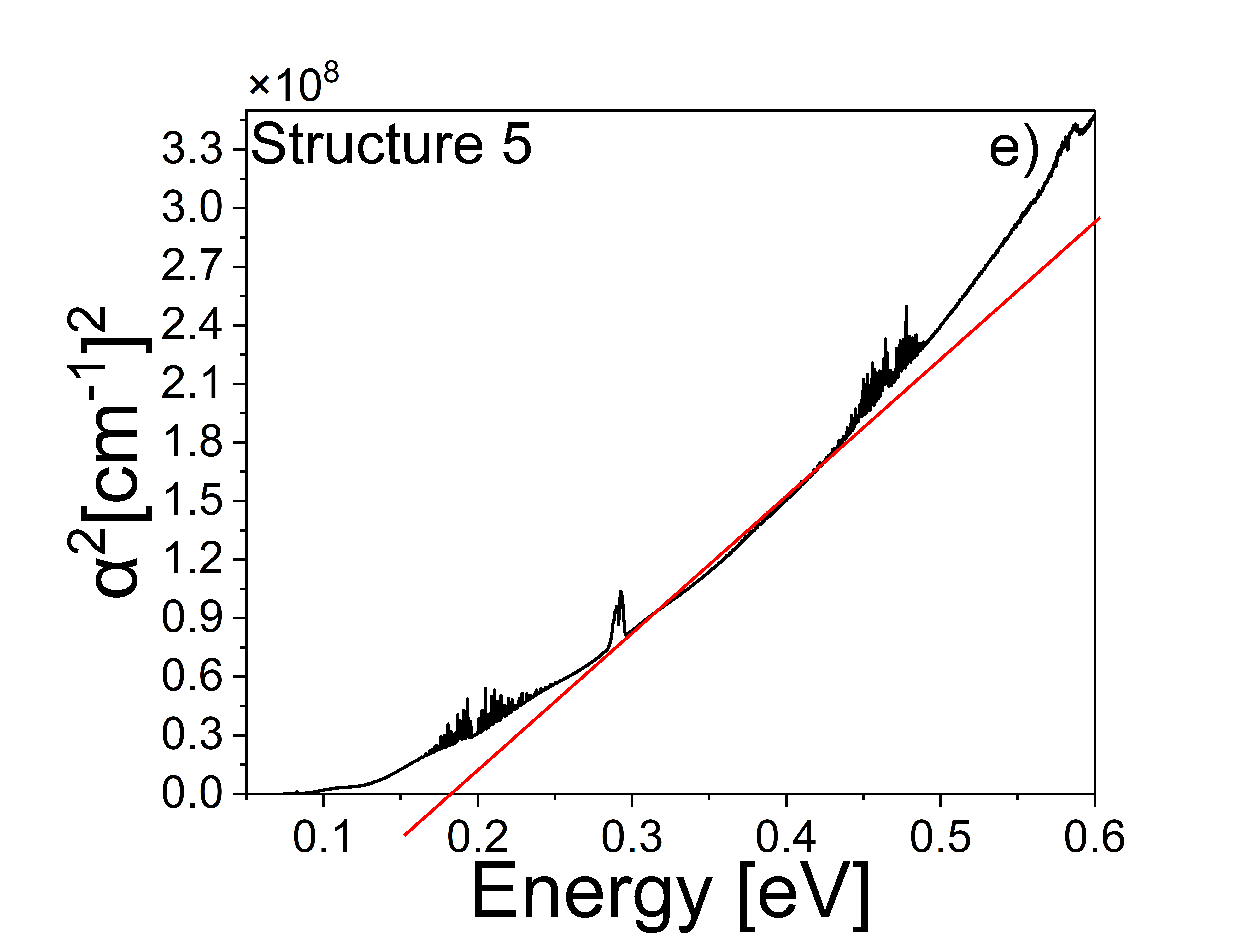
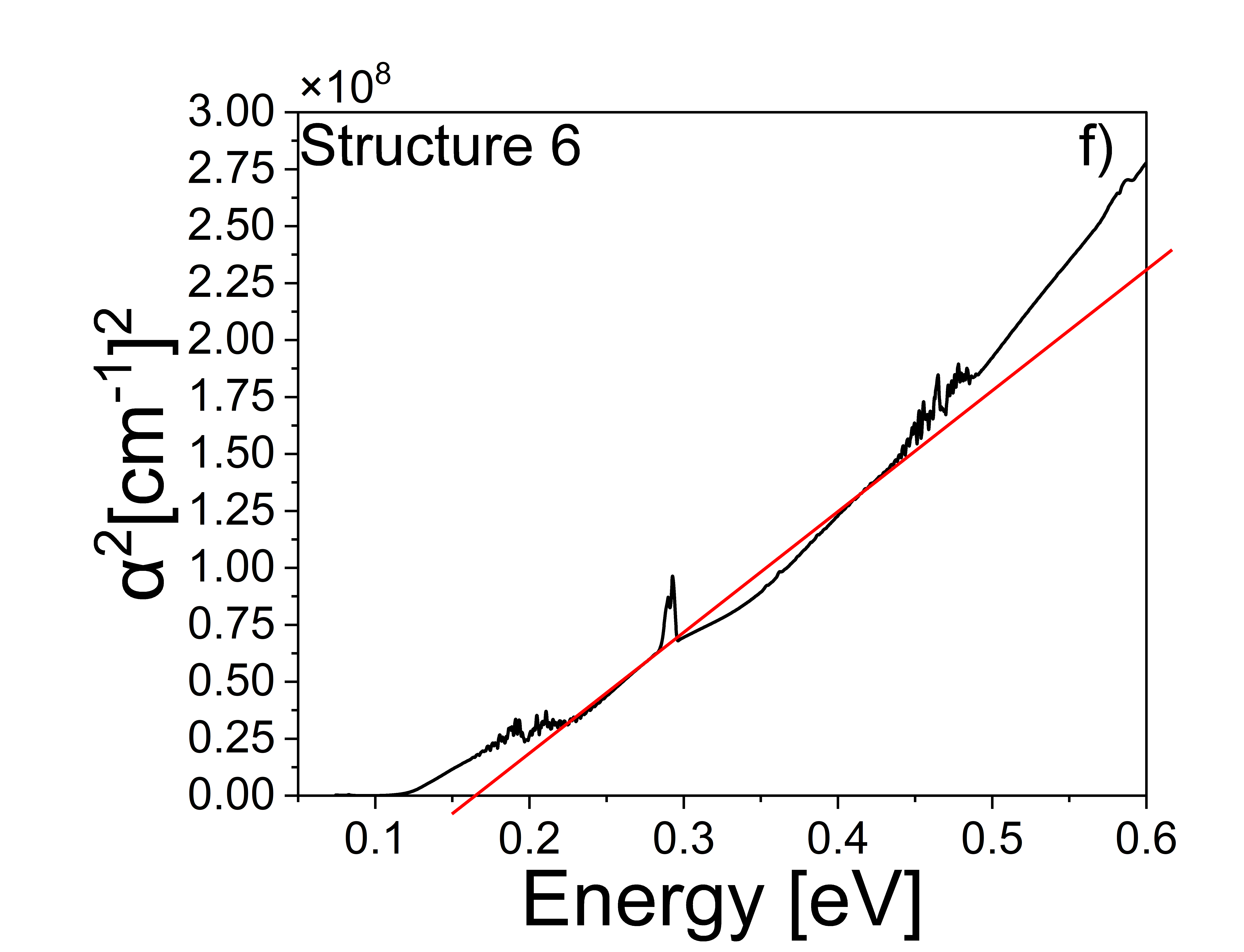
Optical transmission spectra in a wavelength near the energy gap are used also to estimate the x value of Hg1−𝑥Cd𝑥Te. When the value of 𝐸𝑔 is known, it is possible to determine the value of x based on the relationship between the bandgap position and the Cd concentration in the Hg1−𝑥Cd𝑥Te [21]. The most widely used expression approximating E𝑔 (𝑥, 𝑇) due to Hansen et al. [22]: 𝐸𝑔 = −0.302+1.93𝑥−0.81𝑥2+0.832𝑥3+5.35𝑥10-4 (1−2𝑥)𝑇 was used to supplementary verification of determined values. The slight deviations of 𝐸𝑔 values have been observed, but it was not exceeding 0.02 eV in each sample. Structure 6 has the smallest concentration of x = 0.2; Structure 2 has the highest concentration with x = 0.31. In most cases, the composition determined by the optical spectroscopy and XRD measurements is similar. The largest discrepancy at the level of 6% was recorded for Structure 2. The differences may result from many factors like: XRD analyses the crystalline structure, while transmittance studies the optical properties of the material, the presence of defects and heterogeneity, or the influence of the Fermi level position which can cause a shift of the apparent absorption edge to shorter wavelengths. It is worth noting that the additional IR bands and noise present in the spectrum of Structure 5 and Structure 6 come from the vibrations of atmospheric molecules (H2O and CO2).
The objective of this work was to improve the crystalline and optical quality of the Hg1−𝑥Cd𝑥Te layers by adjusting the MBE growth parameters. For this purpose, the authors characterized the effects of the Hg/Te flux ratio and substrate temperature on the structural properties of Hg1−𝑥Cd𝑥Te, producing a series of structures that were grown with Hg/Te flux ratios between 185–200 and substrate temperature between 175–185 °C. Structural and optical characterization was conducted using various analysis techniques, such as XRD rocking curves, FTIR spectroscopy, optical and confocal microscopy, and XRD reciprocal space mapping. These methods provided valuable insight into growth quality, thicknesses, and dislocation density, which are crucial for simulating the optical and device properties of these materials. A Panalytical Empyrean system, equipped with an analyser crystal for high-resolution studies, was employed to examine the XRD in all structures, enabling extensive rocking curve and reciprocal space mapping. A hybrid monochromator was used to measure the triple-axis rocking curves around the primary symmetric reflections of the (422) peaks in the (211)-oriented structures. The minimum value of FWHM𝑅𝐶 of HgCdTe is 21.5 arcsec, and the dislocation density is about 1.35 × 105 cm-2, which indicates the growth of high-quality material. 2D-RSMs around the (422) reciprocal lattice points directly reveal the strain status of the structure layer. All grown structures were found to be under tensile in-plane biaxial strain. Characterizing the surface morphology and related surface defects of MBEgrown structures is crucial because they reflect the crystal growth mechanism during MBE growth. The epilayer surface morphology was influenced by the growth temperature, as shown in Fig. 4(b)–(f), which presents surface images of Hg1−𝑥Cd𝑥Te epilayers grown at different temperatures, observed via Nomarski optical microscopy. It is clear that the optimal growth temperature lies within the lower temperature range, as increasing the growth temperature leads to surface hillock formation and increased surface roughness. Figures 4(c) and (d) indicate good surface quality for epilayers grown at 175 °C, whereas higher growth temperatures resulted in gradually deteriorating surface morphology, despite a constant II/VI flux ratio. The value and variation of the composition x are probably the most important parameter in detector grade. The authors have studied the IR transmission method to determine the Hg1−𝑥Cd𝑥Te layers composition. In most cases, the composition determined by the optical spectroscopy and XRD measurements is similar. The largest discrepancy at the level of 6% was recorded for Structure 2. The differences may result from many factors like: XRD analyses the crystalline structure, while transmittance studies the optical properties of the material, the presence of defects and heterogeneity, or the influence of the Fermi level position which can cause a shift of the apparent absorption edge to shorter wavelengths. In summary, structures with good surface morphology, good crystalline structure, and dislocation density are consistently achieved, and run-to-run reproducibility is very good.
Research concept and design, I.R. and J.G.; collection and assembly of data, I.R.; data analysis and interpretation, M.M., M.R., R.W.-N., I.R. and A.J.; writing the article, I.R. and M.R.; critical revision of the article, T.W. and M.M.
The authors thank Msc. Piotr Krzemiński from Centre for Microelectronics and Nanotechnology for SEM measurements. This researchwas partially supported by the Foundation for Polish Science project "MagTop" no. FENG.02.01- IP.05-0028/23 is cofinanced by the European Union from the funds of Priority 2 of the European Funds for a Smart Economy Program 2021–2027 (FENG).
Sze, S. M. & Lee, M. K. Semiconductor Devices: Physics and Technology, 3rd Edition. (Wiley, New York, 1985).
Lawson, W., Nielsen, S., Putley, E. & Young, A. Preparation and properties of HgTe and mixed crystals of HgTe-CdTe.J. Phys. Chem. Solids 9, 325–329 (1959). https://doi.org.10.1016/0022-3697(59)90110-6
Rogalski, A. Infrared and Terahertz Detectors, Third Edition.(CRC Press, 2019). https://doi.org.10.1201/b2195.
Dvoretsky, S. A. et al. Study of the crystalline state of MBE (013) HgCdTe/CdTe/ZnTe/GaAs heterostructure layers by the second harmonic generation method. Semiconductors 56, 562–569 (2022). https://doi.org.10.21883/SC.2022.08.54114.31
Gu, R. et al. Recent progress in MBE grown HgCdTe mate- rials and devices at UWA. Proc. SPIE 9819, 98191Z (2016). https://doi.org.10.1117/12.2222997.
Madni, I. et al. X-ray reciprocal space mapping of MBE grown HgCdTe on alternative substrates. Cryst. Res. Technol. 52, 1700167 (2017). https://doi.org.10.1002/crat.201700167
Holý, V., Wolf, K., Kastner, M., Stanzl, H. & Gebhardt,W. X-ray triple-crystal diffractometry of defects in epitaxic layers. J. Appl. Crystallogr. 27, 551–557 (1994). https://doi.org.10.1107/s0021889894000208
Carmody, M., Lee, D., Zandian, M., Phillips, J. & Arias, J. Threading and misfit-dislocation motion in molecular-beam epitaxy-grown HgCdTe epilayers. J. Elec- tron. Mater. 32, 710–716 (2003). https://doi.org.10.1007/s11664-003-0057-7.
Koppensteiner, E., Bauer, G., Kibbel, H. & Kasper, E. In- vestigation of strain-symmetrized and pseudomorphic Sim- Gen superlattices by x-ray reciprocal space mapping. J. Appl. Phys. 76, 3489–3501 (1994). https://doi.org.10.1063/1.357478
Holý, V., Kubena, J., Abramof, E., Pesek, A. & Koppen- steiner, E. X-ray diffractometry of small defects in layered systems. J. Phys. D: Appl. Phys. 26, A146–A150 (1993). https://doi.org.10.1088/0034-4885/59/11/001.
Fewster, P. F. X-ray analysis of thin films and multilayers. Rep. Prog. Phys. 59, 1339–1407 (1996). https://doi.org.10.1088/0034-4885/59/11/001.
Sluis, P. Determination of strain in epitaxial semiconductor structures by high-resolution X-ray diffraction. Appl. Phys. A 58, 129–134 (1994). https://doi.org.10.1007/BF00324367.
Hrauda, N. et al. Strain distribution in Si capping layers on SiGe islands: influence of cap thickness and footprint in reciprocal space. Nanotechnology 23, 465705 (2012). https://doi.org.10.1088/0957-4484/23/46/465705
Dolabella, S., Borzì, A., Dommann, A. & Neels, A. Lattice strain and defects analysis in nanostructured semiconductor materials and devices by high-resolution X-ray diffraction: Theoretical and practical aspects. Small Methods 6, 2100932 (2021). https://doi.org.10.1002/smtd.202100932
Bauer, G. & Ritcher, W. Optical Characterization of Epi- taxial Semiconductor Layers. (Springer Berlin Heidelberg, 1996). https://doi.org.10.1007/978-3-642-79678-4.
Sankowska, I. et al. A study of defects in InAs/GaSb type- II superlattices using high-resolution reciprocal space map- ping. Materials 14, 4940 (2021). https://doi.org.10.3390/ma14174940
Sankowska, I. et al. On the onset of strain relaxation in the Al0.45Ga0.55As/In𝑥Ga1−𝑥As active region in quantum cascade laser structures. J. Appl. Crystallogr. 50, 1376–1381 (2017). https://doi.org.10.1107/s1600576717011815
Authier, A., Lagomarsino, S. & Tanner, B. K. X-ray and Neutron Dynamical Diffraction: Theory and Applications, vol. 357 (Springer, New York, 2012).
Fewster, P. F., Andrew, N. L. & Curling, C. J. Interface roughness and period variations in the AlGaAs system grown by molecular beam epitaxy. Semicond. Sci. Technol. 6, 5–10 (1991). https://doi.org.10.1088/0268-1242/6/1/002
Chang, Y. et al. Surface morphology and defect formation mechanisms for HgCdTe (211)B grown by molecular beam epitaxy. J. Electron. Mater. 37, 1171–1183 (2008). https://doi.org.10.1007/s11664-008-0477-5
Rogalski, A. HgCdTe infrared detector material: history, status and outlook. Rep. Prog. Phys. 68, 2267–2336 (2005). https://doi.org.10.1088/0034-4885/68/10/R01.
Hansen, G. L., Schmit, J. & Casselman, T. Energy gap versus alloy composition and temperature in Hg1−𝑥Cd𝑥Te. J. Appl. Phys. 53, 7099–7101 (1982). https://doi.org.10.1063/1.330018