A CROW/MZI-based switch for silicon photonics applications
- Department of Electronics, Nuclear Materials Authority, 4710030 Cairo, Egypt
- Engineering Physics and Mathematics Department, Faculty of Engineering, Ain Shams University, Cairo 11517, Egypt
Article Info
Received 21 Oct. 2024
Received in revised form 06 Dec. 2024
Accepted 09 Dec. 2024
Available on-line 03 Feb. 2025
Keywords: silicon photonics; integrated optics; switching; modulation; ring resonators; Mach-Zehnder interferometer.
Abstract
In this work, the authors propose the design of an electro-optical silicon-photonics hitless switch that follows wavelength-division multiplexing (WDM) conditions in terms of channel bandwidth, shape factor, and free spectral range. Through a careful step-by-step design, the authors study a switch device composed of a coupled-resonator optical waveguide (CROW) structure merged with a Mach-Zehnder interferometer (MZI) modulator. The MZI modulator controls the coupling to the CROW and hence turns the switch on and off. The traditional matrix analysis of the CROW structure is modified to accommodate the MZI modulator section. The proposed switch requires a chip area of less than 0.01225 mm2. The switch transmission satisfies WDM requirements with a channel-free spectral range of 100 GHz, channel flat-top response with a passband for the through/drop ports of 64.6 GHz/33 GHz, and a shape factor of 0.76/0.6. Besides, the switch transmission features an insertion loss for the through/drop ports of 0.23/1 dB, a switching speed of 100 GHz, and a competitive switch-on/off ratio of 33 dB.
Introduction
The progress in integrated optics relies on the development of new optical materials [1–3] and new photonic circuit designs, both in the near-infrared range [4–8] and more recently in the mid-infrared range [9, 10]. To realize optical integrated circuits, researchers have explored various platforms, such as ion exchange in glass [11–13], III-V semiconductors [14], and silicon-on-insulator (SOI) platform [15]. Given its prominence in electronics [16], SOI has become a primary focus for developing integrated optical circuits. The goal is to combine these photonic circuits seamlessly with existing electronic ones, creating high-performance hybrid systems. Specifically, the siliconon- silica platform offers a significant refractive index contrast at the C-band, allowing small bending radii and high-density integration of photonic circuits [17]. Additionally, both silicon and silica possess very low propagation losses at a wavelength of 1550 nm, enabling the realization of effective components like ring resonators [18], interleavers [19, 20], gyroscopes [21], and fibergrating couplers [22].
One key element is optical switches which are indispensable components for high-performance on-chip optical networks [23]. Their ability to handle large bandwidths, low-power consumption, and minimal footprint make them crucial for multi-core microprocessor systems [24]. Thus, in this work, the authors propose a design for a high-speed large-bandwidth hitless switch. The switch consists of three ring resonators with coupling control facilitated by a Mach-Zehnder interferometer (MZI)-based modulator. The modulation is achieved thanks to an electro-optic polymer placed over SOI. The design targets wavelength-division multiplexing (WDM) requirements in terms of channel free spectral range (FSR), 3 dB channel bandwidth and shape factor which are 100 GHz, at least 20 GHz and at least 0.6, respectively. The article is organized as follows. In section 2, the design parameters are determined. In section 3, a transfer matrix analysis is introduced. The results are discussed in section 4 before the authors conclude in section 5.
Design parameters
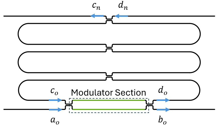
The proposed structure is shown in Fig. 1. The structure is composed of three coupled-ring resonators squeezed between two bus waveguides. This structure is usually referred to in the literature as a coupled-resonator optical waveguide (CROW) structure. The rings take the form of racetracks to simplify the design of the coupling region. Hereinafter, the rings are referred to as “ring 1” for the bottom ring, “ring 2” for the middle ring, and “ring 3” for the top ring. The lower bus has its input port on the left end and its output port, called the through port, on the right end. The other output port in this circuit is the drop port, found on the left end of the top bus. The right port of the top bus is supposed to serve as a second input to the circuit, but it is not used. The lower bus forms an MZI with the lower side of ring 1 alongside two 3 dB directional couplers. This MZI structure controls how much power is coupled from the lower bus into ring 1 by tuning the effective refractive index of the propagating modes in the two arms of the MZI [25]. This means that the switch can be put to the ON state when power is allowed to couple, in a certain amount, from the lower bus into ring 1. In this state, the through and the drop ports are transmitting optical signals. When the MZI is tuned so that no power couples into the bottom ring, the switch is in the OFF state and the drop port has zero transmission, while all input power is directed toward the through port. This coupling modulation technique means that the switching speed is not limited by the photon lifetime in the resonator or the channel FSR [26]. Hence, the limit is set by the modulation mechanism only. This also means that the switch provides hitless operation since the drop port signal can be disabled without disturbing the original signal on the through port, an advantage for WDM operation [27].
Multiple modulation techniques can be used to achieve coupling modulation in silicon to get around its poor electro-optic coefficient [28–30]. One technique could be the thermal tuning of the silicon refractive index thanks to its good thermo-optic coefficient. However, thermal modulation is relatively slow [28–30]. Next comes plasma injection and extraction in silicon waveguides. Introducing or removing free carriers (electrons and holes) can alter the waveguide refractive index. Injection-based devices offer a strong refractive index change, leading to compact size and low operating voltage. However, such devices suffer from electrical DC loss, high optical absorption, and limited bandwidth due to carrier lifetime constraints [31]. Depletion-based devices [32–36] are preferred due to their high speed, zero DC loss, and low optical losses. Yet, an attractive alternative, which the authors adopt in this work, is modulating the coupling using electro-optic polymers, specifically CLD1/APC [37]. Due to its high electro-optic coefficient, this material grabbed much attention in modulation applications [37, 38]. The design in [38] shows the polymer on top of a silicon-on-silica waveguide with all layers eventually sandwiched between two electrodes. The device is designed to operate around free space wavelength, λo, of 1550 nm. The effective refractive index, ne, responds to the tuning voltage as given by dne/ dV = −2.48 ×10⁻⁴/V where V is the voltage applied to one arm of the MZI modulator. This is about one magnitude greater response than in plasma extraction-based modulators [33].
Thus, based on the structure in [38] and the WDM requirements given in [39], the rest of the device parameters are determined as follows. At 1550 nm, ne = 2.159 and the group refractive index, ng, is equal to 4.11 [38]. To determine the circumference, L, the WDM condition on the FSR, is equal to 100 GHz around 1550 nm. This FSR is equal to 0.8 nm in terms of wavelength [39]. Therefore, the ring circumference is L = c /(ng × FSR) = 729.5 μm, where c = 3 × 10⁸ m/s is the speed of light in space. The authors adopt the power loss factor in [38], which is α = 6 dB/cm. This means an optical power loss of approximately 10% for one cycle around the ring. This power loss matches also the assumption in [39]. The authors also adopt the number of rings to be three in order to simplify the structure while satisfying the WDM requirements. For a waveguide-waveguide separation, g, of 0.2 μm, the coupling length is l = 9.75 μm [40]. This is the interaction length of each of the two adjacent waveguides in a directional coupler to enable 100% power coupling from one waveguide to the other. The field coupling coefficient is given by k = sin(Lw × π/2l ). Thus, for a 3 dB directional coupler, k2 = 0.5, and hence the interaction length is found as
\( L_w=\frac{2 l}{\pi} \sin ^{-1}(\sqrt{0.5})=4.87 \mu \mathrm{~m} \)
One can also define
\( r=\sqrt{1+k^2} \)
as the field through coupling coefficient. Thus, the authors allow more length for the 3 dB directional coupler structure, so that its share of the ring circumference is 10 μm to account for the S-bends around the coupling region of the coupler. Thus, on the lower side of the bottom racetrack, a length of 20 μm is dedicated for the 3 dB couplers. A similar length is assumed on the other side of the racetrack. However, away from the bottom bus, coupling is enabled through one directional coupler that requires an interaction length less than 20 μm. The extra length can be exhausted in the S‑bends. The power coupling coefficient for two neighbouring rings is 0.39, while for ring 1 or ring 3 and the neighbouring bus it is 0.8. These two coupling coefficients result in interaction lengths of 4.18 μm and 6.87 μm, respectively, for g = 0.2 μm. Recall that the coupling between ring 1 and the lower bus is controlled through the MZI modulator. Hence, when the tuning voltage is zero (ON state), the MZI should provide a power coupling of 0.8, i.e., k = 0.8 , between ring 1 and the lower bus. When the modulating voltage is applied (OFF state), the coupled power should drop to zero. Therefore, only ring 3 and the top bus require a directional coupler of length 6.87 μm. It is noteworthy to mention that having a gradually changing coupling coefficient throughout the structure, known as “apodization”, is needed to reduce the transmission side lobes and to enhance the flat transmission band [39]. The bending radius is taken as R = 5 μm for negligible bending losses [40]. Finally, the MZI arm length, LMZI, is found from
\( L_{\mathrm{MZI}}=0.5 \times(L-4 \times 10 \mu \mathrm{~m}-2 \pi R)=329 \mu \mathrm{~m} . \)
This is the allowed length for modulation and consequently, along with the desire phase shift, it determines the required tuning voltage, V. The design parameters are summarized in Table 1.
Table 1.
Summary of the device parameters.
Parameter |
Value |
Free space wavelength λo |
1550 nm |
Effective refractive index at λo = 1550 nm, ne |
2.159 |
Group refractive index at λo = 1550 nm, ng |
4.11 |
Power loss factor α |
6 dB/cm |
Ring circumference L = c/(ngFSR) |
729.5 μm |
MZI arm length LMZI |
329 μm |
Bend radius R |
5 μm |
Ring-ring power coupling coefficient |
0.39 |
Ring-bus power coupling coefficient |
0.8 |
Device footprint |
400 μm × 40 μm |
Transfer matrix analysis
Let the number of rings in the switch be n. Then, n = 3 for the structure shown in Fig. 1. The input field is given by ao, the through port field by bo, and the drop port field by cn = c3. The other input field is dn = d3 = 0. The goal now is to determine the normalized through field transmission, ρo= bo/ao and the normalized drop field transmission, τo = c3/ao . The MZI section has input and output electric fields on the ring side given by co and do, respectively. The MZI fields can be related through [25, 41]:
\( b_o=x_1 a_o+x_2 c_o \) (1)
\( d_o=x_3 a_o+x_4 c_o \) (2)
where
\( x_1=-x_4=0.5\left(e^{-i \theta_1}-e^{-i \theta_2}\right) \) (3)
\( x_2=x_3=-0.5 i\left(e^{-i \theta_1}+e^{-i \theta_2}\right) \) (4)
\( \theta_1=\frac{2 \pi}{\lambda_o} L_{M Z I}\left(V \frac{d n_e}{d V}\right)+\Phi_1 \) (5)
\( \theta_2=\frac{2 \pi}{\lambda_0} L_{M Z I}\left(-V \frac{d n_e}{d V}\right)+\Phi_2 \) (6)
Here, V is the voltage applied to one arm of the MZI modulator, LMZI, the Mach-Zehnder arm length, ne is the effective refractive index of the propagating mode, λo is the free space wavelength. The two parameters θ1 and θ2 give the propagation phase change through the upper arm and the lower arm of the MZI, respectively. Besides, Φ1 and Φ2 are the constant phase shifts added to each of the two arms of the MZI. This is different from the traditional analysis given in [25, 41] where the phase shift in one arm is met with its negative in the other arm. Therefore, traditionally with Φ1 = Φ2 = 0, the MZI parameters change to
\( x_1=-x_4=-i \sin \left(\frac{2 \pi}{\lambda_o} L_{\mathrm{MZZ}}\left(V \frac{\mathrm{~d} n_e}{\mathrm{~d} V}\right)\right) \)
and
\( x_2=x_3=-i \cos \left(\frac{2 \pi}{\lambda_o} L_{\mathrm{MZI}}\left(V \frac{\mathrm{~d} n_e}{\mathrm{~d} V}\right)\right) \)
This means that when the applied voltage is zero, 100% of the power couples between lower bus and ring 1. This does not yield the desirable WDM channel transmission characteristics as shown in [39]. Providing specific power coupling is where the authors’ work departs from the classic work in [25, 41]. Also, in [25, 41], the switch has only one output port and the switch turns off when the coupling changes to the critical coupling condition. In the authors’ work, the switch is turned off by reducing the coupling to zero. This allows the hitless operation where the through port keeps transmitting and the drop port shuts down. For acceptable transmission, the power coupling coefficient is 0.8 and this can be satisfied by shifting the phase in each arm by a constant value which is achieved through a very small extra length added to each arm. The authors found that the right phase shift values are Φ1 = 2 rad and Φ2 = 1.11 rad. The corresponding extra lengths are 0.23 μm and 0.12 μm, respectively. Such small lengths will effectively not affect the FSR of the rings. Equations (1) and (2) can be put in the form:
\( \left[\begin{array}{l} a_0 \\ b_0 \end{array}\right]=X\left[\begin{array}{l} c_0 \\ d_0 \end{array}\right] \) (7)
where
\( X=\frac{1}{x_3}\left[\begin{array}{cc} -x_4 & 1 \\ x_2 x_3-x_1 x_4 & x_1 \end{array}\right] \) (8)
Thus, matrix X is the matrix that relates to the electric fields of the MZI section. The rest of the analysis can be done using the well-known technique in [42], with the modification of using the MZI X matrix driven above. Then, the fields in the two buses are related through:
\( \left[\begin{array}{l} a_o \\ b_o \end{array}\right]=M\left[\begin{array}{l} d_n \\ c_n \end{array}\right]=\left[\begin{array}{ll} M_{11} & M_{12} \\ M_{21} & M_{22} \end{array}\right]\left[\begin{array}{l} d_n \\ c_n \end{array}\right] \) (9)
Matrix M is given by:
\( M=X P\left(\prod_{j=1}^{n-1} Q_j P\right) Q_n \) (10)
with
\( Q_j=\frac{1}{i k_j}\left[\begin{array}{ll} r_j & -1 \\ 1 & -r_j \end{array}\right] \) (11)
\( P=\left[\begin{array}{cc} 0 & e^{-\frac{i \delta}{2}} \\ e^{\frac{i}{2}} & 0 \end{array}\right] \) (12)
where α is the power loss factor, δ = 2πne/ λo , L-iαL/2 represents the complex phase change for one complete round, Q is (3) (4) (5) (6) M. Elkattan, M. Gad /Opto-Electronics Review 33 (2025) e153810 4 the coupling matrix and P is the phase matrix. Here, k1 = k2 = √0.39 and k3 = kn = √0.8. Note that in a classical analysis, X = Qo with 3 ko = k3 = √0.8. Using dn = 0, one finally gets:
\( \rho_o=\frac{M_{22}}{M_{12}} \) (13)
\( \tau_o=\frac{1}{M_{12}} \) (14)
Results and discussion
The device performance is shown in Fig. 2. With V = 0, typical transmission characteristics for the through and the drop ports are shown. The through/drop ports show insertion loss (IL) of 0.23 dB/1 dB, 3 dB bandwidth (BW) of 64.6 GHz/33 GHz (equivalently 0.516 nm/0.264 nm), crosstalk (CT) of −19 dB/-20 GHz within 20 GHz of the channel centre wavelength, and shape factor (S) of 0.74/0.6. The shape factor is defined as the ratio of the −1 dB BW to the −10 dB BW [39]. The channel spacing is given by FSR = 0.8 nm or equivalently 100 GHz. The channel bandwidth, the shape factor, and the FSR all meet the WDM requirements [39].
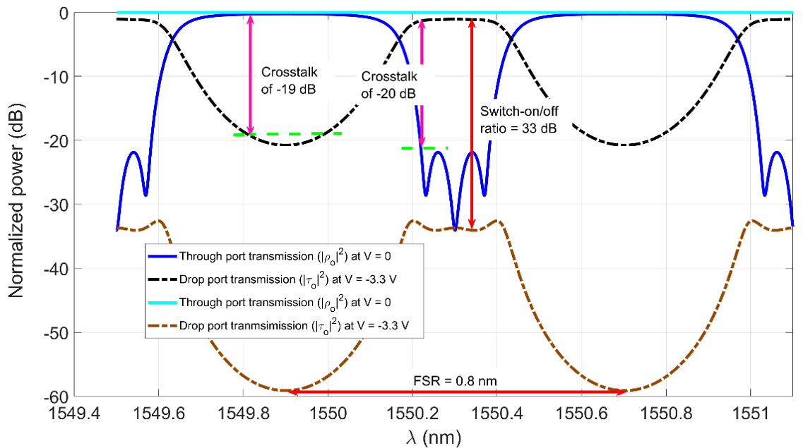
When tuning voltage V = 3.3 V is applied to the bottom arm of the MZI modulator and its negative value to the top arm, the drop port becomes OFF by at least 33 dB below its transmission level in the ON state. This is the switchon/ off ratio. Again, in the OFF state, the drop port only shuts down while the regular channels on the through port keep transmitting without change constituting the hitless switch operation. The speed of operation is independent of the photon lifetime since it is based on coupling modulation rather than frequency modulation. Therefore, the switching speed can reach 100 GHz. Finally, with all these advantageous performance metrics, the device requires less than 350 μm × 35 μm = 0.01225 mm2 of chip area.
The advantages of the proposed design become clearer when compared to other designs. In the pioneering work presented in [41], amplitude modulation is used in a III-V platform switch. However, only one ring is used, hence, the transmission characteristics take a typical Lorentzian shape without regard to WDM requirements on BW, S, or FSR. As mentioned above, the switch has one output only, through the port, where power turns on and off as amplitude modulation turns between maximum coupling, i.e., 100% power coupling and critical coupling. The reported switching time is 1.8 μs due to relying on thermal tuning, which is too slow compared to the proposed design.
In another interesting work [43], an SOI second-order switch, i.e., with two resonators, is demonstrated. The device employs a vertical PN junction as the tuning mechanism. Electric current is turned on and off to switch the structure at a 2.4 ns speed. The drop port BW is 40 GHz, the drop port switch-on/off ratio, called extinction ratio in [43], is 25 dB and the device is compact with a disk radii of 3 μm each. Again, the WDM requirements are not a focus in that work and the switching speed is much less than the proposed one. Besides, both channels, the through and drop, get turned on and off together, which is not a hitless operation.
In Ref. [44], a quadruple SOI multi-channel hitless switch is demonstrated. The switching mechanism is thermo-optical, which limits the speed to 15 μs. Using four rings of course enhances the transmission extinction ratio, reported as 39–46 dB, and the CT reported as 19.3–24.5 dB. The FSR is equal to 0.5 nm, which is less than the WDM specification of 0.8 nm.
In Ref. [45], a 4 × 4 SOI hitless router is demonstrated where each of the eight 10 μm radius rings is thermally tuned to route the optical signal. The device footprint is 0.07 mm2. The reported extinction ratio is 20.79 dB, FSR is 38.5 GHz and switching speed is in the range of microseconds. These results are less efficient compared to our proposed design.
In [46], an SOI CROW of five apodized rings is used. The laser is focused on a spot in the structure to inject free carriers to turn the switch on and off. The footprint is, the 40 × 12 μ2 switching speed is less than 2 ns (still slower than the proposed design and the extinction ratio is limited to 10–17 dB (while the authors’ is in the range of 33 dB). Besides, using the laser in tuning the switch adds more complexity to the system design.
In [47], a p-i-n lateral diode is used to switch the 10th order switch on and off with a 100 GHz passband and a 10 dB switch-on/off ratio. The switching speed is 1 ns. While this switch has good performance, the switch-on/off ratio and the switching speed are not competitive compared to the authors’ design.
In [24], a review of more recent designs is provided. The switches operate using electro-optical or thermo-optical mechanisms. The switching speed ranges from 41 ns to 76 μs. The footprint ranges from 0.0058 mm2 to 0.0225 mm2. The IL ranges from 0.5 dB to 9 dB. The CT ranges from −11.5 dB to −41.7 dB. This review shows the trade-off between design parameters where, for example, a more box-like transmission comes at the expense of footprint. It also shows that the proposed design possesses competitive characteristics with state-of-the-art designs.
A comparison of the current work with other designs is provided in Table 2. In Table 2, the advantages of the proposed work manifest themselves in different aspects, such as operating BW, FSR, and S. The switching speed for the authors’ design is also clearly higher than that for other devices, especially those that rely on the thermo-optic tuning mechanism.
Table 2.
A comparison of the proposed design with work in literature.
Ref. |
Platform |
Device footprint |
Switching speed |
Hitless operation |
Switching mechanism |
Transmission profile |
[45] |
SOI |
0.07 mm2 |
1 μs |
Yes |
Thermo-optic |
BW = 38.5 GHz |
[48] |
SOI |
NA |
NA |
No |
Thermo-optic |
BW = 0.12 to 2.91 nm |
[43] |
SOI |
Rings with 3 μm radius |
2.4 ns |
No |
PIN junction |
BW = 40 GHz CT = −25 dB FSR = 4.2 THz |
[49] |
SOI |
NA |
Rise time < 12.5 ns Fall time < 6.1 ns |
No |
PIN junction |
BW = 31 nm CT = −20 dB |
[50] |
SOI |
4.6 × 2 mm2 |
64 Gb/s |
No |
PIN junction |
BW = 60 nm CT = −19.4 dB |
This work |
SOI |
0.01225 mm2 |
100 GHz |
Yes |
Electro-optic polymer on SOI |
FSR = 100 GHz For the through/drop channels: BW = 64.6/33 GHz Switch-on/off ration 33 dB IL = 0.23/1 S = 0.76/0.6 |
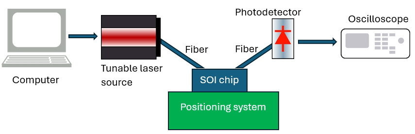
Finally, to characterize the proposed switch, the authors can use a measurement system like the one shown in their previous work [20]. A simplified optical diagram for such a setup is shown in Fig. 3. In this setup, a tunable near-infrared laser source with a central wavelength of λo = 1550 nm is used as the source of radiation. A computer is used to tune the wavelength through the range of measurements. The source is vertically coupled to an optical fibre that couples light into the SOI chip via on-chip grating couplers. These grating couplers allow only trnsverse electrics (TE) field modes and eliminate other polarizations as in [20]. Power is received on the other end of the chip through a similar mechanism, where an optical fibre couples power out of the chip and into the photodetector. A 3D positioning system is used to align the fibres and the chip to achieve the right power coupling position to decrease power losses in the measurement system. The transmission profiles are then shown on an oscilloscope.
Conclusions
A detailed design is proposed for an electro-optical switch that considers the WDM conditions on channel BW, S, and FSR. The design uses coupling modulation to eliminate the photon lifetime limitation on the switching speed in a hitless operation. The matrix analysis of the CROW structure is modified to accommodate the MZI coupling modulator. Combining all these ideas results in a competitive switch with very high speed, low CT, high switch-on/off ratio, low IL, and WDM-compatible BW and FSR.
Authors’ statement
Research concept and design, M.G.; collection of data, M.E.; assembly of data, M.G.; data analysis and interpretation, M.E.; writing the article, M.E. and M.G.; critical revision of the article, M.E.; final approval of article, M.G. and M.E.
References
-
Gad, M. & Elkattan, M. Tailoring the optical properties of polyvinyl alcohol-polyvinyl pyrrolidone based polymers. Opt. Quantum Electron. 55, 985 (2023). https://doi.org/10.1007/s11082-023-05233-6
-
Elkattan, M. & Gad, M. Tuning the optical constants of PVA based films for optoelectronic applications. Opt. Commun. 527, 128979 (2023). https://doi.org/10.1016/J.OPTCOM.2022.128979
-
Elkattan, M. & Gad, M. Investigation of the absorption edge and the optical bandgap of PVA/PVP-based thin films. J. Electron. Mater. 54, 831–847 (2024). https://doi.org/10.1007/s11664-024-11536-5
-
Mahrous, H. et al. A multi-objective genetic algorithm approach for silicon photonics design. Photonics 11, 80 (2024). https://doi.org/10.3390/photonics11010080
-
Mahrous, H., Fedawy, M., Abboud, M., Selim, D. & Gad, M. Optimizing the Design of a Silicon-Photonics Interleaver Circuit. in 2022 39th National Radio Science Conference (NRSC) 293–300 (IEEE, 2022). https://doi.org/10.1109/NRSC57219.2022.9971168
-
Shalaby, R. A. et al. Silicon Photonic Coupled-Ring Resonator in Nested Configuration Comprising Different Length Scales. in 14th International Conference on Computer Engineering and Systems (ICCES) 432–437 (IEEE, 2020). https://doi.org/10.1109/icces48960.2019.9068163
-
Shalaby, R. A. et al. Silicon photonics dual-coupler nested coupled cavities. Proc. SPIE 10923, 109231P (2019). https://doi.org/10.1117/12.2509661
-
Elkattan, M. & Gad, M. A high-speed silicon-photonics WDM switch for optical networks applications. Photonics 11, 1115 (2024). https://doi.org/10.3390/photonics11121115
-
Labib, M., Gad, M., Sabry, Y. M. & Khalil, D. Optimization of silicon on silica waveguides for mid-infrared applications at 4.28 um. Proc. SPIE 10923, 109231H (2019). https://doi.org/10.1117/12.2508079
-
Labib, M., Gad, M., Sabry, Y. M. & Khalil, D. Strip Waveguide Enabling Low Loss for Silicon on Silica Technology in the MIR. in 13th International Conference on Computer Engineering and Systems (ICCES) 536–540 (IEEE, 2018). https://doi.org/10.1109/ICCES.2018.8639316
-
Monir, M., El-Refaei, H. & Khalil, D. Single-mode refractive index reconstruction using an NM-line technique. Fiber Integr. Opt. 25, 69–74 (2006). https://doi.org/10.1080/01468030500466230
-
Monir, M., El-Refaei, H., Khalil, D. & Omar, O. A. Assessment of the NM-lines sensitivity for measurement errors. Fiber Integr. Opt. 26, 1–15 (2007). https://doi.org/10.1080/01468030601000250
-
Gad, M., El-Refaei, H., Khalil, D. & Omar, O. A. Comparison of the N times mode-lines technique to the inverse technique in refractive index profile reconstruction. Opt. Eng. 46, 094601 (2007). https://doi.org/10.1117/1.2785177
-
Hu, Y., Liang, D. & Beausoleil, R. G. An advanced III-V-on-silicon photonic integration platform. Opto-Electron. Adv. 4, 2000094 (2021). https://doi.org/10.29026/oea.2021.200094
-
Ferraro, F. J. et al. Imec silicon photonics platforms: Performance, overview and roadmap. Proc. SPIE 12429, 1242909 (2023). https://doi.org/10.1117/12.2650579
-
Mahrous, H., Fedawy, M., El Sabbagh, M., Fikry, W. & Gad, M. Design of a 90 GHz SOI fin electro-optic modulator for high-speed applications. Appl. Sci. 9, 4917 (2019). https://doi.org/10.3390/app9224917
-
Bogaerts, W. et al. Silicon microring resonators. Laser Photonics Rev. 6, 47–73 (2012). https://doi.org/10.1002/lpor.201100017
-
Gad, M., Yevick, D. & Jessop, P. A comparison of modeling methods for ring resonator circuits. J. Opt. Soc. Am. A 27, 703–708 (2010). https://doi.org/10.1364/josaa.27.000703
-
Gad, M., Yevick, D. & Jessop, P. Compound ring resonator circuit for integrated optics applications, J. Opt. Soc. Am. A 26, 2023–2032 (2009). https://doi.org/10.1364/josaa.26.002023
-
Gad, M., Ackert, J., Yevick, D., Chrostowski, L. & Jessop, P. Ring resonator wavelength division multiplexing interleaver. J. Light. Technol. 29, 2102–2109 (2011). https://doi.org/10.1109/JLT.2011.2157081
-
Gad, M., Yevick, D. & Jessop, P. High sensitivity ring resonator gyroscopes. Fiber Integr. Opt. 30, 395–410 (2011). https://doi.org/10.1080/01468030.2011.611581
-
Gad, M., Zaki, A. & Sabry, Y. M. Silicon Photonic Mid-Infrared Grating Coupler Based on Silicon-on-Insulator Technology. in 2017 34th National Radio Science Conference (NRSC) 400–406 (IEEE, 2017). https://doi.org/10.1109/NRSC.2017.7893509
-
Xie, Y. et al. Towards large-scale programmable silicon photonic chip for signal processing. Nanophotonics 13, 2051–2073 (2024). https://doi.org/10.1515/nanoph-2023-0836
-
Yue, W., Cai, Y. & Yu, M. Review of 2 × 2 silicon photonic switches. Photonics 10, 564 (2023). https://doi.org/10.3390/photonics10050564
-
Yariv, A. Critical coupling and its control in optical waveguide-ring resonator systems. IEEE Photonics Technol. Lett. 14, 483–485 (2002). https://doi.org/doi:10.1109/68.992585
-
Li, G.et al. Ring resonator modulators in silicon for interchip photonic links. IEEE J. Sel. Top. Quantum Electron. 19, 95–113 (2013). https://doi.org/10.1109/JSTQE.2013.2278885
-
Lira, H. L. R., Manipatruni, S. & Lipson, M. Broadband Hitless Silicon Electro-Optic Switch for Optical Networkson-Chip. in 2009 6th IEEE International Conference on Group IV Photonics 253–255 (IEEE, 2009). https://doi.org/10.1109/GROUP4.2009.5338366
-
Reed, G. T., Mashanovich, G., Gardes, F. Y. & Thomson, D. J. Silicon optical modulators. Nat. Photonics 4, 518–526 (2010). https://doi.org/10.1038/nphoton.2010.179
-
Cocorullo, G., Iodice, M., Rendina, I. & Sarro, P. M. Silicon thermooptical micromodulator with 700-kHz-3-dB bandwidth. IEEE Photonics Technol. Lett. 7, 363–365 (1995). https://doi.org/10.1109/68.376803
-
Gardes, F. Y., Reed, G. T., Emerson, N. G. & Png, C. E. A sub- micron depletion-type photonic modulator in silicon on insulator. Opt. Express. 13, 8845–8854 (2005). https://doi.org/10.1364/opex.13.008845
-
Krishnanunni, R. A. & Ravindran, S. Investigating the performance of a novel silicon based p-i-n modulator with enhanced carrier injection. Opt. Quantum Electron. 56<, 1359 (2024). https://doi.org/10.1007/s11082-024-07284-9
-
Mahrous, H. et al. Design of compact, high-speed and low-loss silicon-on-silica electro-optic modulators. Semicond. Sci. Technol. 35, 095017 (2020). https://doi.org/10.1088/1361-6641/ab9d09
-
Mahrous, H., Fedawy, M., El Sabbagh, M., Fikry, W. & Gad, M. A compact 120 GHz monolithic silicon-on-silica electro-optic modulator. Opt. Quantum Electron. 52 1–11 (2020). https://doi.org/10.1007/s11082-020-2239-4
-
Mahrous, H., Fedawy, M., El Sabbagh, M., Fikry, W. & Gad, M. 130 Gbps low-loss electro-optic modulator based on metal-oxide- semiconductor technology. Optik (Stuttg) 217, 164928 (2020). https://doi.org/10.1016/J.IJLEO.2020.164928
-
Mahrous, H., Fedawy, M., Abboud, M., Selim, D. & Gad, M. Optimizing the Design of a Silicon-Photonics Interleaver Circuit. in 2022 39th National Radio Science Conference (NRSC) 293–300 (IEEE, 2022).
-
Mahrous, H., Gad, M., El Sabbagh, M., Fedawy, M. & Fikry, W. A High-Speed Electro-Optic Modulator with Optimized Electrode Positions. in 2018 13th International Conference on Computer Engineering and Systems (ICCES) 530–535 (IEEE, 2018). https://doi.org/10.1109/ICCES.2018.8639436
-
Rabiei, P., Steier, W. H., Zhang, C. & Dalton, L. R. Polymer micro- ring filters and modulators. J. Light. Technol. 20, 1968–1975 (2002). https://doi.org/10.1109/JLT.2002.803058
-
Gad, M., Yevick, D. & Jessop, P. E. Tunable polymer/silicon over insulator ring resonators. Opt. Eng. 47, 124601 (2008). https://doi.org/10.1117/1.3050355
-
Kaalund, C. J. & Peng, G.-D. Pole-zero diagram approach to the design of ring resonator-based filters for photonic applications. J. Light. Technol. 22, 1548–1559 (2004). https://doi.org/10.1109/JLT.2004.824526
-
Gad, M., Yevick, D. & Jessop, P. E. High-speed polymer/silicon on insulator ring resonator switch. Opt. Eng. 47, 094601 (2008). https://doi.org/10.1117/1.2978947
-
Green, W. M. J., Lee, R. K., DeRose, G. A., Scherer, A. & Yariv, A. Hybrid InGaAsP-InP Mach-Zehnder racetrack resonator for thermooptic switching and coupling control. Opt. Express 13, 1651 (2005). https://doi.org/10.1364/opex.13.001651
-
Cho, S.-Y. & Soref, R. Interferometric microring-resonant 2 × 2 optical switches. Opt. Express 16, 13304–13314 (2008). https://doi.org/10.1016/B978-0-12-803581-8.09769-1
-
Watts, M. R., Trotter, D. C. &. Young, R. W. Maximally Confined High-Speed Second-Order Silicon Microdisk Switches. in NationalFiber Optic Engineers Conference 2008 PDP14 (Optical Publishing Froup, 2008).
-
Goebuchi, Y., Hisada, M., Kato, T. & Kokubun, Y. Optical cross- connect circuit using hitless wavelength selective switch. Opt.Express 16, 535 (2008). https://doi.org/10.1364/oe.16.000535
-
Sherwood-Droz, N. et al. Optical 4 × 4 hitless silicon router for optical networks-on-chip (NoC): erratum. Opt. Express 16, 19395 (2008). https://doi.org/10.1364/oe.16.019395
-
Vlasov, Y., Green, W. M. J. & Xia, F. High-throughput silicon nanophotonic wavelength-insensitive switch for on-chip optical networks. Nat. Photonics 2, 242–246 (2008). https://doi.org/10.1038/nphoton.2008.31
-
Luo, X. et al. Silicon high-order coupled-microring-based electro- optical switches for on-chip optical interconnects. IEEE Photonics Technol. Lett. 24, 821–823 (2012). https://doi.org/10.1109/LPT.2012.2188829
-
Chen, W. et al. Flexible-grid wavelength-selective switch based on silicon microring resonators with interferometric couplers. J. Light. Technol. 36, 3344–3353 (2018). https://doi.org/10.1109/JLT.2018.2839665
-
Konoike, R., Suzuki, K., Ikeda, K. & Paper, T. Path-independent insertion loss 8 × 8 silicon photonics switch with nanosecond-order switching time. J. Light. Technol. 41, 865–870 (2023). https://doi.org/10.1364/JLT.41.000865
-
Lu, L. et al. Silicon non-blocking 4 × 4 optical switch chip integrated with both thermal and electro-optic tuners. IEEE Photonics J. 11, 1– 9 (2019). https://doi.org/10.1109/JPHOT.2019.2941960