An electronic control system developed by our team for spatial mapping in Raman spectroscopy integrated with a glove box is described in this article. Key features include a Positioning and Optical Preview System with a 3-axis NanoMax stage for precise sample mapping, a Control Module based on the STM32F207 microcontroller for managing stage movements and synchronisation, and a custom software solution enabling measurement synchronisation via TTL signals. To validate our Raman mapping methodology, we analysed mechanically ground α-MoO₃ powder deposited on glass. The acquired spectra clearly exhibited all the characteristic vibrational modes of the orthorhombic phase, confirming the reliability of our mapping technique.
Introduction
Raman spectroscopy is an advanced analytical technique that reveals the structural, chemical, and physical properties of a wide range of materials, including nanomaterials, semiconductors, polymers, and biomolecules [1–5]. This method is widely applied across numerous fields, including physics, chemistry, materials science, pharmaceuticals, biology, and geology, due to its ability to provide detailed molecular insights in a non-destructive manner. Its versatil-ity and precision make it an indispensable tool for both fundamental research [6–9] and industrial applications [10].
Unfortunately, most Raman spectrometers currently available on the market are engineered to operate exclu-sively under atmospheric conditions, requiring samples to be analysed in ambient air. This limitation can be particularly problematic for materials that are highly susceptible to environmental factors, such as humidity, oxygen, or temperature changes. For instance, exposure to ambient conditions can lead to oxidation, hydration, or structural degradation in sensitive samples, potentially compromising the accuracy and reliability of the analysis. As a result, there is a growing need for advanced Raman systems capable of operating in controlled environments, such as vacuum or inert-gas chambers, to ensure the integrity of samples and expand the applicability of this powerful technique. While cryostat-based systems have addressed some of these challenges by enabling vacuum and cryogenic measurements, our innovative glove box-integrated spectrometer provides a superior solution for room-temperature investigations of air-sensitive materials. Unlike cryostats, which require vacuum or extremely low temperatures, our system operates at ambient pressure and temperature within an inert atmosphere, making it uniquely suited for investigating materials that may undergo phase transitions or property changes under extreme conditions. The primary advantage of our approach is the combination of spectroscopic characterisation with full sample accessibil-ity. Whereas cryostats restrict physical manipulation once the sample is mounted, our system allows real-time in situ processing – including chemical treatments, electro-chemical modifications, and device fabrication – while maintaining a controlled environment. This capability is especially valuable for studying dynamic processes in energy storage materials, catalytic systems, and metastable phases that require room-temperature analysis. Moreover, our design overcomes the spatial constraints typical of most cryostats by accommodating significantly larger samples and enabling true macroscopic Raman mapping. The system supports correlative characterisation by integrating optical microscopy with Raman spectroscopy, providing direct compatibility with standard sample preparation tools. This eliminates the need for potentially damaging transfers between fabrication and measurement stations. From a practical perspective, experimental efficiency is signifi-cantly improved by glove box integration by eliminating the lengthy pump-down and thermal equilibration times required by cryostats. It maintains exceptional environ-mental control without introducing thermal drift artifacts that can complicate spectral interpretation in variable-temperature measurements. This technological innovation fills a crucial niche in materials characterisation, particularly for two-dimensional materials, hybrid perovskites, and other vacuum-incompatible systems, as well as surface reactions requiring real-time monitoring and large-area samples that need comprehensive mapping. Our system complements, rather than replaces, cryogenic Raman capa-bilities – offering researchers a versatile tool for room-temperature studies of air-sensitive materials under realistic experimental conditions. By bridging the gap between conventional atmospheric and cryogenic measurements, this design enables the exploration of material properties that were previously inaccessible to Raman spectroscopy.
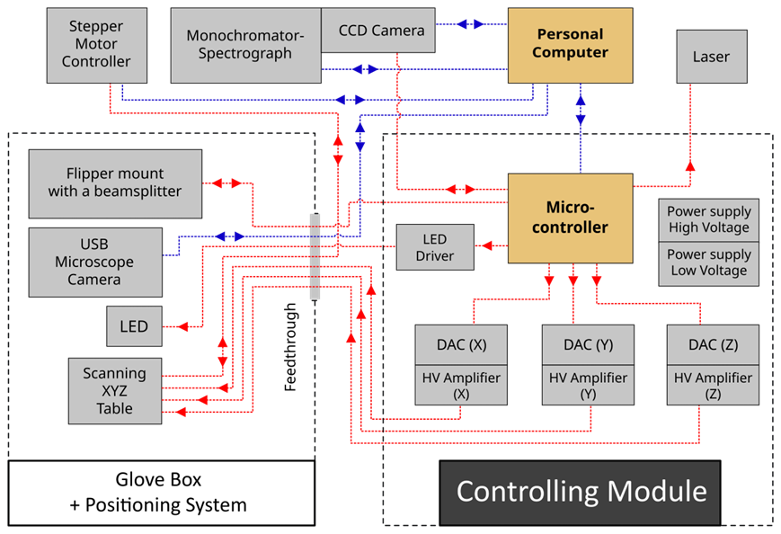
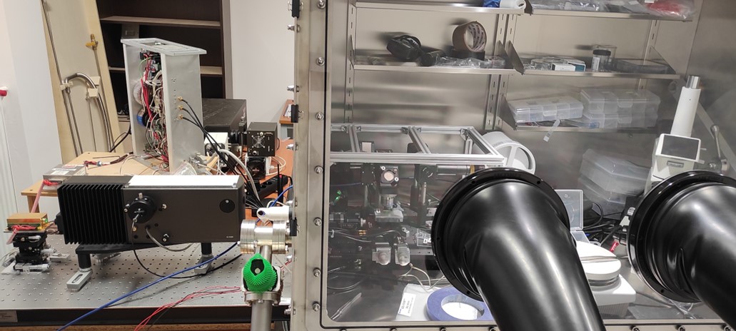
In our previous article, the successful integration of a Raman spectrometer with a glove box was outlined, highlighting the benefits of this setup through comprehen-sive testing [11]. Our findings revealed that measurements conducted under argon atmosphere are significantly more reliable and reproducible compared to those performed in ambient air, emphasizing the critical role of controlled environments for accurate analysis. This article provides an in-depth exploration of a custom-designed electronic control system developed by our team specifically for Raman mapping applications in the glove box. The system is engineered to generate precise control signals for the positioning stage, enabling the creation of detailed spatial maps during Raman spectroscopy measurements. By integrating complex control mechanisms, this approach significantly improves the accuracy and versatility of the Raman analysis. However, to achieve the intended func-tionality, the device structure must be divided into modules using a dedicated design approach. Fig. 1 shows a block diagram of our integration of a glove box with a Raman spectrometer. This setup is particularly focused on the control methods for the stage used in mapping samples. The glove box provides a controlled environment for handling sensitive materials, while the Raman spectrometer is used to analyse the molecular composition of the samples. The control mechanism for the stage is essential for the precise positioning and mapping of the samples to ensure accurate and reliable spectroscopic data collection. Fig. 2 displays a photograph of our integration setup of a Raman spectrometer with a glove box. Three main components are included in the setup: (1) the glove box (Jacomex GP Campus), (2) the Positioning and Optical Preview System installed inside the glove box, (3) the MS5204i spectrometer (SOL Instruments) featuring a Czerny-Turner optical design with a 520 mm focal length equipped with a thermoelectrically-cooled CCD detector (Hamamatsu HS 101H-2048/122-HR2), and the Raman module (SOL Instruments).
Fig. 2.Raman spectrometer coupled with a glove box
Mapping system
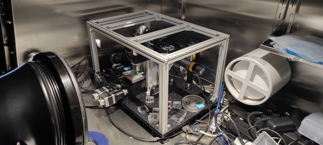
As part of the Raman system development, we designed and built the Positioning and Optical Preview System, which is mounted in the glove box, as illustrated in Fig. 3. In the system, to mount optical components, a 30 × 50 cm² optical breadboard with a 30 mm rod-spacing cage system (Thorlabs Inc.) are used. The laser beam is directed to the objective lens (Zeiss LD EC Epiplan-Neofluar 50 ×/0.55 HD DIC M27) via adjustable mirrors, focusing precisely on the sample surface. Scattered light is collected by the same objective and directed back outside the glove box for analysis. The core of the system is a 3-axis NanoMax stage (Thorlabs Inc.), equipped with stepper and piezoelectric actuators enabling independent movement along the x-, y‑, and z-axes. Coarse movement (0–4 mm range, 2 μm accuracy) is achieved using stepper motors, while piezo-electric actuators control fine movement (0–20 μm range) for mapping. This setup, combined with the optical preview capabilities, allows for precise sample positioning and area selection and facilitates high-accuracy Raman mapping.
Fig. 3.The Positioning and Optical Preview System installed in
the glove box.
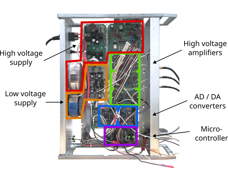
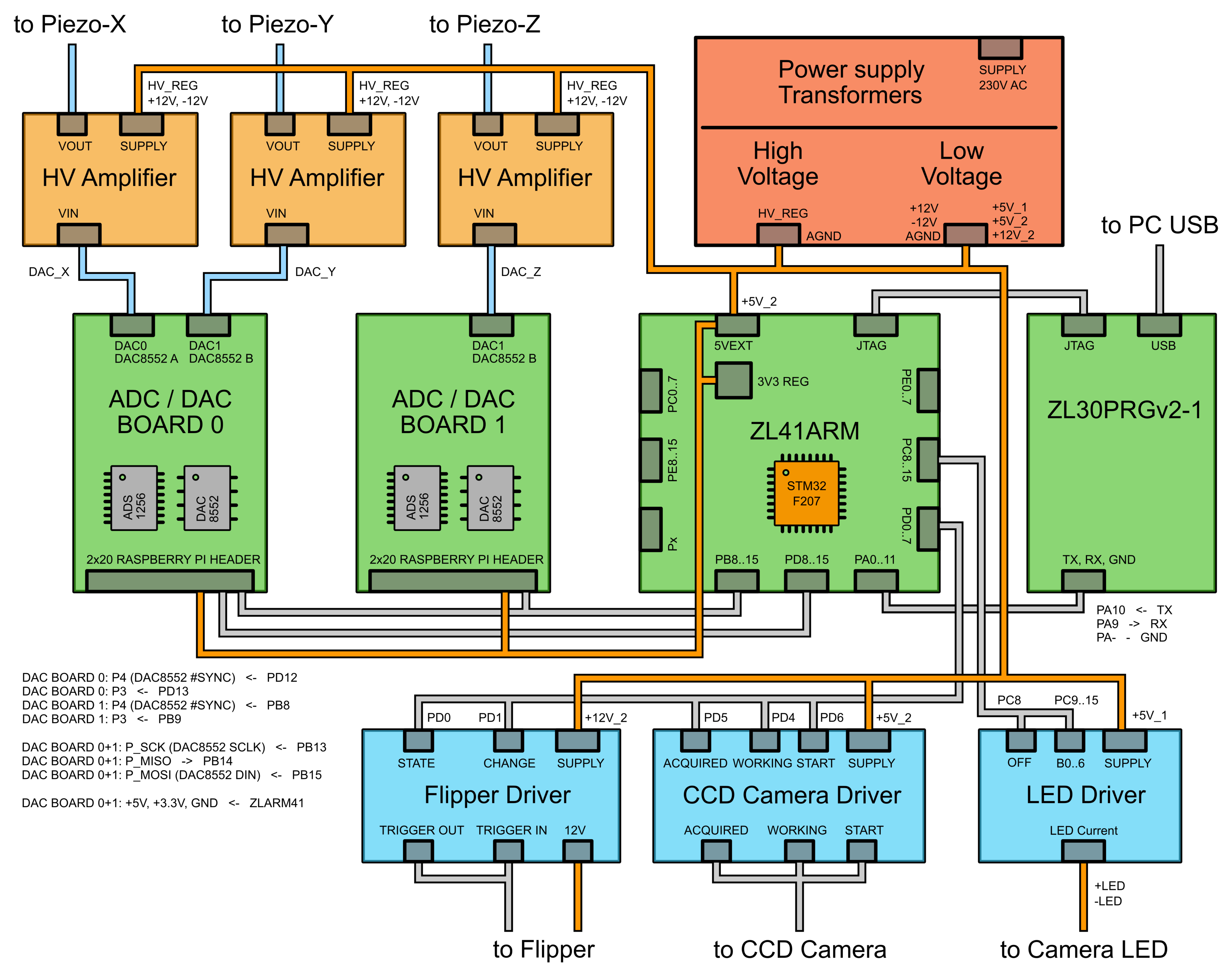
One of the most critical functionalities implemented in our system is sample positioning during measurement, enabling precise Raman mapping using a 3-axis NanoMax stage. The Raman mapping measurements are conducted using a NanoMax positioning stage equipped with internal piezoelectric actuators operating in open-loop control mode along the x-, y-, and z-axes. As specified by the manufacturer, this stage offers a 20 μm travel range with a + 0.2 μm tolerance along all three axes, achieving a theoretical resolution of 10 nm in the x-, y-, and z-directions. The system exhibits 200 nm bidirectional repeatability and maintains an absolute on-axis accuracy of 1.0 μm throughout its operational range. These precision engineering specifications enable high-resolution spatial mapping while ensuring reliable and reproducible positioning for confocal Raman measurements. Thus, a controlled sample movement along the x-, y-, and z-axes, ensuring accurate spatial mapping of the sample surface is provided by this system. By combining coarse positioning (achieved via stepper motors) with fine adjustments (enabled by piezoelectric actuators), the system enables both wide-area selection and high-resolution mapping – essential for detailed analysis of material properties and structures. In our configuration, the measurement setup components are PC-controlled, while a dedicated Control Module supervises all remaining components. Fig. 4 shows the Control Module with its functional blocks highlighted. The module main components include:
Fig. 4.Control Module with highlighted functional blocks,
entirely designed and constructed by our team.
32-bit STM32F207 microcontroller with an ARM Cortex-M3 core (STMicroelectronics). The embedded software was developed in C using GNU Tools for ARM Embedded Processors (version 7.2.1).
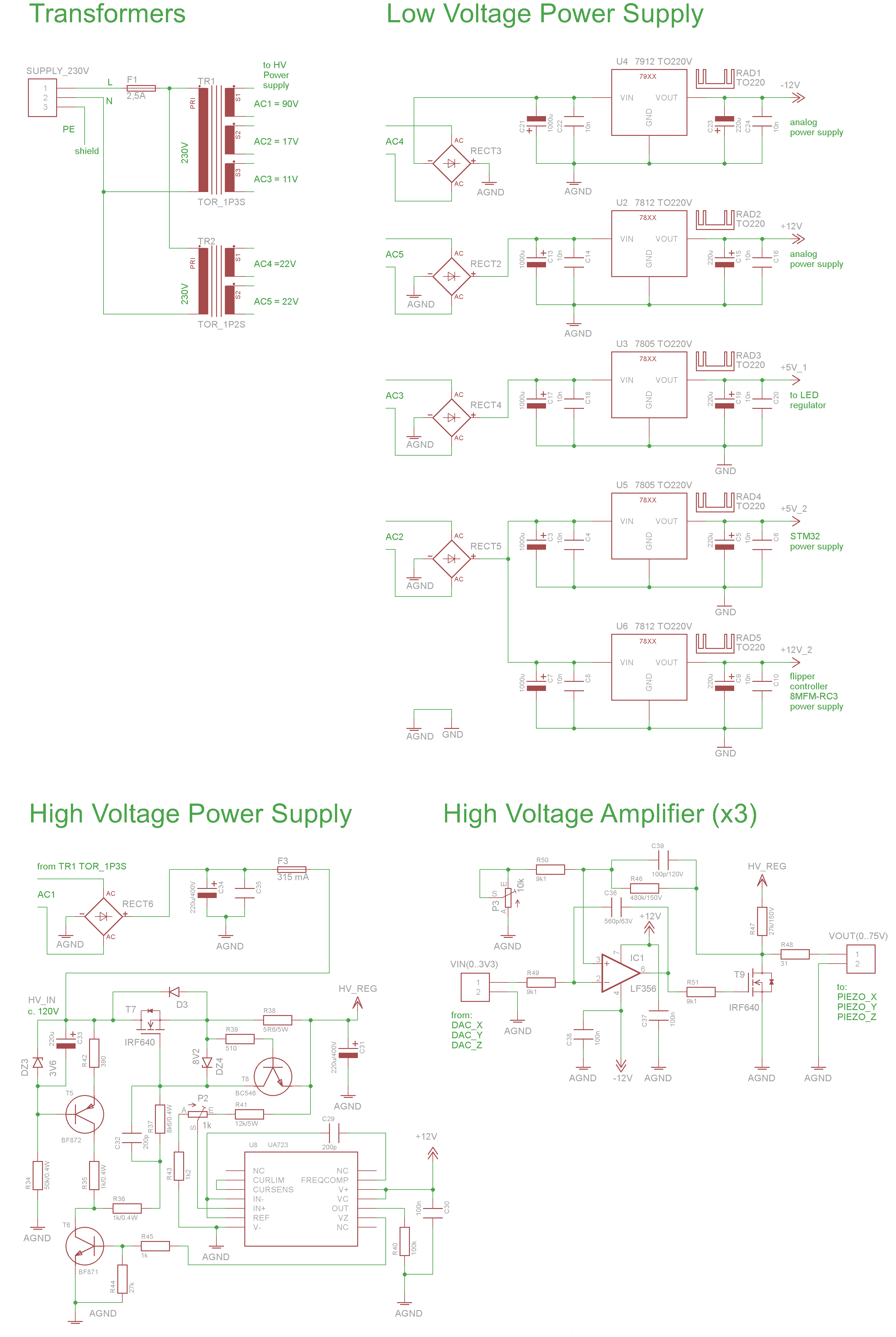
16-bit digital-to-analogue converters (DAC8552, Texas Instruments) convert digital control signals into analogue voltages (0–3.3 V) for precise movement control of the x-, y-, and z-axis piezoelectric actuators.
High-voltage amplifiers (HVAs) boost the DAC8552 output signals from 0–3.3 V to the 0–75 V range required for piezoelectric actuator operation.
100 V high-voltage (HV) power supply for the amplifiers and a separate low-voltage power supply for the remaining electronic circuits.
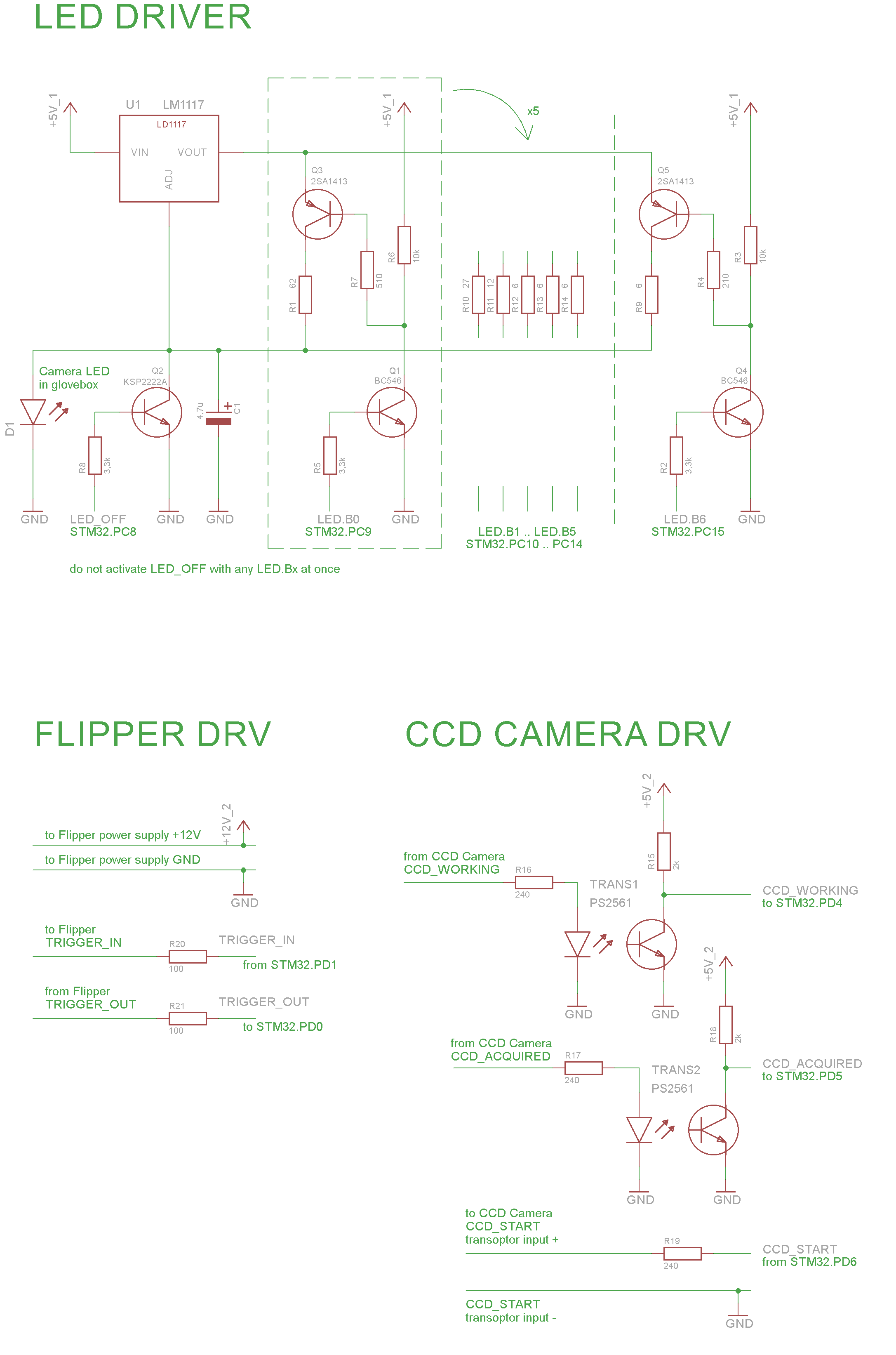
Peripheral circuits handle multiple control functions, including LED illuminator current regulation, movable arm (flipper) actuation, CCD camera (spectrum detector) communication, and laser power switching (on/off). These circuits typically use single-transistor open-collector configurations with opto-isolation for reliable operation
The SpectraSP software (SOL Instruments), designed exclusively for monochromator and CCD camera control, lacks native mapping capabilities or XYZ stage control. To overcome this limitation, a solution leveraging the CCD camera external TTL triggering capability was developed. In our approach, synchronised operation of two PC applications is implemented, enabling precise coordination between sample positioning and spectral acquisition. By this workaround, the system functionality is effectively extended beyond the manufacturer software constraints, facilitating advanced Raman mapping as detailed below:
The SpectraSP software performs three primary functions: (1) controlling the monochromator and Raman spectroscopy module, (2) acquiring spectral data from the CCD camera, and (3) saving collected spectra as individual files on the host PC. Communica-tion with both the monochromator and CCD camera is established through dedicated Ethernet interfaces.
The second program, RamanMaps (developed by our team), runs on the PC and communicates with the STM32 microcontroller via a USB interface using the CDC communication device class. In this program, commands are sequentially executed to control system devices, including positioning the sample platform (XYZ axes via piezoelectric actuators), adjusting the movable arm, switching the LED illuminator and laser on/off, initiating and monitoring CCD camera acquisition, and verifying the storage of new spectrum files by SpectraSP.
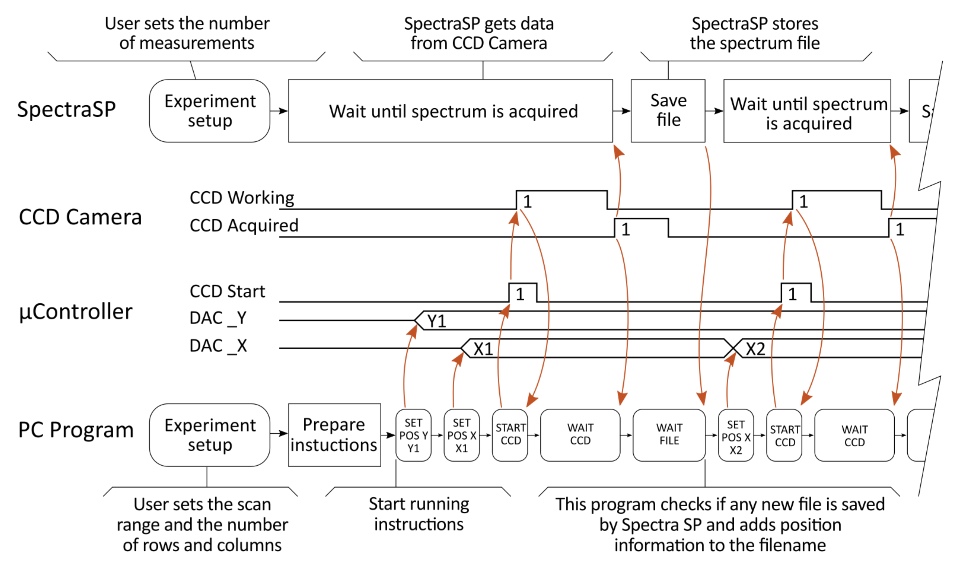
Since the spectrum acquisition triggered by an external TTL signal is supported by the CCD camera, our system synchronises Raman measurements with predefined XYZ sample positions. This mapping implementation is illustrated in Fig. 5. The measurement process begins by configuring parameters in both programs, followed by the generation of a command sequence. While most commands are sent to the microcontroller, certain instructions (e.g., ‘WAIT_FILE’) are executed entirely on the PC.
Fig. 5.Schematic diagram of the measurement process showing the synchronised Raman spectrum acquisition and sample positioning.
To achieve stable, high-resolution measurements while eliminating synchronisation errors and electromechanical response delays, a dedicated measurement protocol was developed. The implemented synchronisation method for coordinated Raman spectrum acquisition and XYZ sample positioning follows this sequence:
Send the command “SET_POS_X VALUE” (or for the Y or Z axis) to the microcontroller, which sets the voltage on the digital-to-analogue converter. This voltage is then amplified and used to drive the piezoelectric element, causing the sample stage to move along the selected axis.
Send the command “START_CCD” to the micro-controller, by which the “CCD Start” signal is activated. The CCD camera then begins the process of collecting the spectrum.
The start of acquisition is confirmed by the CCD camera by activating the “CCD Working” signal. The microcontroller can then complete the execution of the “START_CCD” command initiated in step 2. The acquisition time depends on the settings in the SpectraSP program.
SpectraSP waits for the CCD camera to finish collecting the spectrum. During this time, the “WAIT_CCD” command is sent independently to the microcontroller, placing it in a waiting state until the acquisition is complete.
Once the spectrum is collected, the “CCD Acquired” signal is activated by the CCD camera. SpectraSP retrieves the spectrum, while the active state of the “CCD Acquired” signal is registered by the micro-controller which completes the execution of the command from step 4.
The RamanMaps program on the PC begins executing the “WAIT_FILE” command, which involves monitor-ing the directory containing the spectra. When a new file appears, information about the current X, Y, and Z positions is appended to its filename.
This entire sequence is repeated for each point on the map. In addition to traditional XY mapping, measurements can be performed at several selected points, along arbitrary cross-sections, or along a chosen line in any of the XYZ dimensions. The total measurement time is primarily deter-mined by the acquisition time of a single spectrum multiplied by the number of points. Additional delays (ranging from a few milliseconds to two seconds) arise from various factors, such as:
The time required to transmit commands to and from the microcontroller
The movement time of the piezoelectric actuators.
Delays related to the CCD camera operation cycle.
Delays in detecting a new spectrum file on the computer disk.
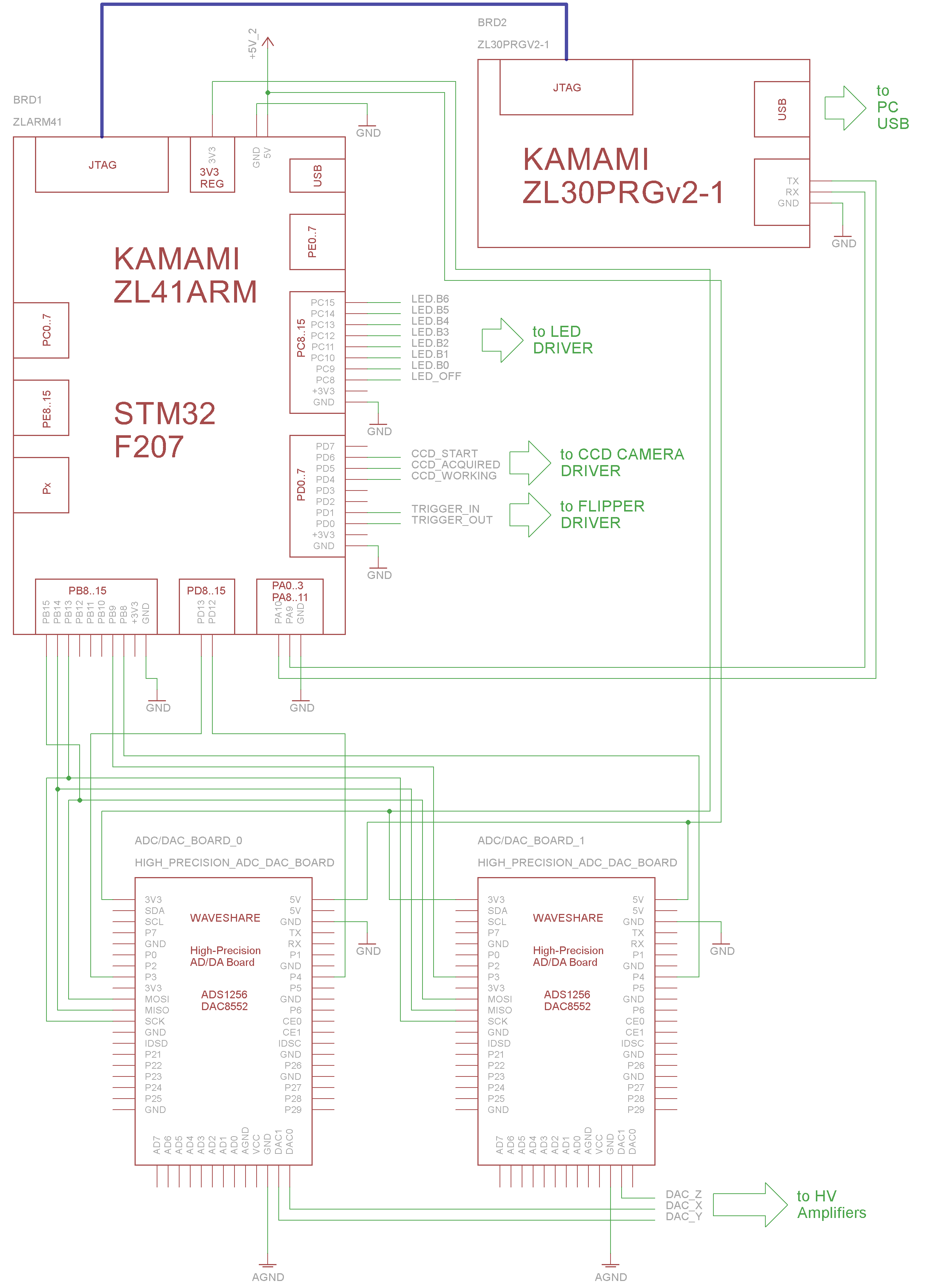
The set of files containing the spectra, along with their corresponding XYZ positions, can be converted into data structures readable by other popular data processing programs, such as ImageJ [12]. Additionally, the files can be converted to a 32-bit TIFF format and analysed in any software, including ImageJ. The details of the electrical connections between the ZL41ARM single-board computer with an STM32F207 microcontroller, the ZL30PRGv2-1 SWD programmer/ debugger for STM32 microcontrollers, and two modules – each featuring a 16-bit dual-channel DAC8552 digital-to-analogue converter and a 24-bit 8-channel ADS1256 analogue-to-digital converter – can be found in the Supporting Information, along with the electrical schematic of the low- and high-power supply circuits and the associated high-voltage amplifier section, and the electrical schematic of the circuits for the LED driver, flipper driver, and CCD camera driver.
Results
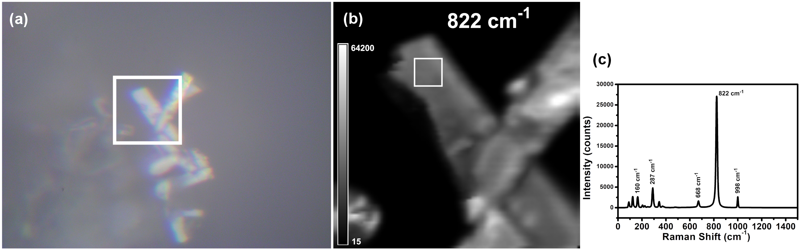
To characterise the performance of our glove box-integrated Raman spectrometer, spatially resolved measure-ments on molybdenum trioxide (MoO₃) powder deposited on a glass substrate were conducted. We employed Raman mapping over a 20 × 20 μm² area using a 100 × 100-point grid (200 nm step size), enabling comprehensive evaluation of the system spatial resolution, signal stability, and detection sensitivity under controlled atmospheric condi-tions. The measurements were performed using a NanoMax positioning stage, which provides an exceptional mechani-cal precision with 20 μm travel range and ~ 10 nm resolution. While the stage nanometer-level positioning capability is critical, the ultimate spatial resolution of our Raman mapping was governed by optical diffraction limits rather than mechanical constraints alone. For our optical configuration – featuring a Zeiss LD EC Epiplan-Neofluar 50×/0.55 NA objective with 532 nm excitation – the theoretical diffraction-limited resolution was calculated as 590 nm laterally (0.61λ/NA) and 2.46 μm axially (1.4nλ/NA² in air). To optimise the measurement con-ditions, several key parameters were implemented: a 100 μm confocal pinhole to enhance signal throughput and improve the signal-to-noise ratio for weak Raman scattering, and a 200 nm scanning step size that exceeds the Nyquist sampling requirement (~ 300 nm for our 590 nm lateral resolution). This configuration provided an optimal balance between spatial fidelity, detection sensitivity, and measurement efficiency, allowing a complete 20 × 20 μm² area mapping while maintaining excellent positional stability. The system capability to resolve subtle spectral variations across the entire scanning area with high spatial precision was demonstrated by the MoO₃ test measure-ments. The choice of MoO₃ as a sample was based on its well-defined Raman-active modes, which serve as a reliable reference for instrument calibration and perfor-mance validation [13–15].
Additionally, MoO₃ is a wide bandgap semiconductor recognised as one of the most promising anisotropic two-dimensional materials [16]. Its rare combination of visible-range quasi-transparency and intrinsic electrical conductivity makes it particularly appealing for modern optoelectronic technologies. The material distinctive electronic structure and layered archi-tecture enable its integration into a broad range of advanced applications, including resistive switching memory devices, photovoltaic systems, birefringent optical elements, and flexible electronics [17]. MoO₃ is of particular interest in our research due to its role as a transition metal oxide (alongside others, such as Re₂O₇) in modifying the work function of graphite [18, 19] and graphene [9, 20–23]. The aim of these studies is to develop transparent conductive anodes for organic light-emitting diodes (OLEDs). Transition metal oxides, such as MoO₃, are promising candidates for enhancing charge injection and improving the efficiency of optoelectronic devices. Fig. 6(a) shows an optical micrograph of MoO₃ powder (prepared by mechanical grinding of bulk crystals) deposited on a glass substrate. The layered orthorhombic structure of α-MoO₃ is evident from the observed flake-like morphology, suggesting partial formation of nanosheets during grinding. The white rectangle indicates the area selected for Raman mapping (20 × 20 μm² scanning area, 100 × 100-point grid). Fig. 6(b) shows a Raman intensity map of the 822 cm−¹ mode (600 lines/mm grating, 2 s spectrum acqui-sition time, 3 mW laser power at 532 nm excitation). Employing these optimised parameters, the complete dataset was obtained in 7 h with a 2.5-s time per point, achieving both high spatial resolution and sufficient signal-to-noise ratio for a reliable phase identification. Fig. 6(c) shows the averaged spectrum from the mapped region demarcated by the white rectangle in Fig. 6(b), with characteristic vibrational modes labelled to confirm the α‑MoO₃ phase identification. In α-MoO₃, the prominent Raman peaks at approximately 822 and 998 cm⁻¹ are characteristic of the orthorhombic phase. These peaks correspond to Mo–O stretching vibrations along the chain axis and terminal Mo=O bonds, respectively. The band around 668 cm−¹ is attributed to the stretching vibration of triply coordinated oxygen atoms (Mo₃–O), reflecting structural connectivity within the MoO₆ octahedra and sensitivity to interlayer coupling. In α-MoO₃ thin films, the same prominent Raman peaks at ~ 822 and ~ 998 cm−¹ remain clear indicators of the α-phase. The 668 cm−¹ band is again associated with the stretching of triply coordinated oxygen.
Fig. 6.(a) Optical micrograph of the MoO₃ powder deposited on a glass substrate. The white rectangle marks the region selected for Raman mapping. (b) Raman intensity map (20 × 20 μm² area, 100 × 100-point grid) of the pristine MoO₃ powder, illustrating the spatial distribution of the phonon mode at 822 cm−¹. The inset shows the scale bar, indicating the corresponding Raman signal intensity values across the sample. (c) Averaged Raman spectrum from the white marked area in (b), with characteristic for α-MoO₃
peaks labelled accordingly
In the low-frequency region, two significant Raman modes are typically observed at approximately 160 cm−¹ and 287 cm−¹. The mode near 160 cm−¹ arises from interlayer shear vibrations, involving the relative sliding motion of adjacent MoO₃ layers along the c-axis, perpendicular to the van der Waals gap. This mode is susceptible to thickness, becoming significantly weaker in ultrathin samples due to reduced interlayer interactions. The 287 cm−¹ mode corresponds to bending vibrations of Mo–O–Mo bridges within the layers. It can shift under mechanical strain, making it a useful probe of internal stress or structural disorder. Our results are fully consistent within experimental error when compared to measurements on powder samples, demonstrating the reproducibility of the observed α-MoO₃ signatures [14, 15], as well as those reported for α-MoO₃ nanoplates [24], and α-MoO₃ nanofibers [25]. For the specified spectrometer confi-guration in our test measurement (520 mm focal length, 600 grooves/mm grating, 100 μm slit width, and 12 μm pixel CCD), the estimated spectral resolution at 532 nm excitation is 5.5 cm−¹ FWHM, as determined through line calibration on a silicon standard reference sample. Our performance on α-MoO₃ validation confirms that their glove box-integrated system is well-suited for sensitive materials research that requires both nanoscale spatial resolution and controlled atmospheric conditions. The combination of precise mechanical control, optimised optical parameters, and systematic mapping protocol ensures reliable characterisation of sample heterogeneity while operating in an oxygen- and moisture-free environment.
Conclusions
The developed system – a glove box-integrated Raman spectrometer – represents an advanced solution for high‑precision spatial mapping under inert-atmosphere conditions. In this unique configuration, are combined measurement accuracy with operational flexibility while maintaining full compatibility with standard analytical workflows. The key technical achievements include:
Positioning and Optical Preview System: a positioning and optical preview system was designed and built, enabling precise sample mapping in Raman spectro-scopy. In the system are included: optical breadboard, adjustable mirrors, objective lens, and 3‑axis NanoMax stage, which provides both coarse and fine movements (controlled by stepper motors and piezoelectric actu-ators).
Precise sample mapping: thanks to the integration of a 3-axis NanoMax stage with piezoelectric actuators, the system allows for accurate sample positioning along the x-, y-, and z-axes, which is crucial for creating detailed spatial maps in Raman analysis.
Control Module: we entirely designed a Control Module based on the STM32F207 microcontroller that manages the stage movements, controls the LED light source and laser, and communicates with the CCD camera. The digital-to-analogue converters and high-voltage amplifiers are used in the module to control the piezoelectric actuators.
Due to the lack of built-in mapping functionality in the SpectraSP software, a solution based on the synchro-nisation of two programs: SpectraSP (for controlling the monochromator and CCD camera) and RamanMaps (for controlling sample positioning and measurement synchronisation) was developed.
Measurement synchronisation: the measurement process is synchronised using TTL signals, allowing for precise correlation between the sample position and the spectral data. Each point on the map is measured sequentially, and the data is saved along with the corresponding XYZ position information.
Measurement flexibility: the system enables not only traditional XY mapping but also measurements at selected points, along cross-sections, or along lines in three dimensions (XYZ).
Measurement time: the total measurement time is primarily dependent on the acquisition time of a single spectrum and the number of points on the map. Additional delays may occur due to data transmission, piezoelectric actuator movements, and the CCD camera operation cycle.
Data analysis: an existing ImageJ plugin was modified to enable the visualisation and analysis of Raman mapping data, enhancing compatibility with widely used image-processing tools.
To validate their Raman mapping methodology, the α‑MoO₃ powder prepared by mechanical grinding and deposited on a glass substrate was analysed. The measured spectra exhibited all characteristic vibrational modes of the orthorhombic phase: strong 822 cm−¹ (chain-axis Mo–O stretching) and 998 cm−¹ (terminal Mo=O stretching) modes, 668 cm−¹ band (Mo₃–O stretching vibration), and low-frequency modes at 160 cm−¹ (interlayer shear) and 287 cm−¹ (in-plane Mo–O–Mo bending). The persistence of these layer-sensitive modes confirms the retention of the layered structure despite mechanical processing, while the complete spectral signature validates our spatial mapping approach for α-MoO₃ characterisation.
The source code for the STM32F207 microcontroller is available upon reasonable request to the corresponding author.
Authors’ statement
Research concept and design, hardware development, M.P.; software development, M.P and Ł.R.; tests and validation, M.P., M.R., P.D., I.L., W.K., M.L.S., and P.K.; writing the article, M.P. and P.K.; critical revision of the article, P.K. and P.J.K.; final approval of article, P.K. and P.J.K.
Acknowledgements
The authors would like to thank Prof. Wielisław Olejniczak for his valuable assistance and expert support in designing the electronic circuits.
This work was supported by the National Science Centre, Poland (grant no. 2017/26/E/ST4/00987) and by the University of Lodz under the IDUB interdisciplinary research grant (no. 2/IGB/2022).
References
Chandra, A. et al. Unveiling the molecular secrets: A comprehensive review of Raman spectroscopy in biological research. ACS Omega 9, 50049–50063 (2024). https://doi.org/10.1021/acsomega.4c00591
Zhang, X., Tan, Q.-H., Wu, J.-B., Shi, W. & Tan, P.-H. Review on the Raman spectroscopy of different types of layered materials. Nanoscale 8, 6435–6450 (2016).
Allakhverdiev, E. S. et al. Spectral insights: Navigating the frontiers of biomedical and microbiological exploration with Raman spectroscopy. J. Photochem. Photobiol. B 252, 112870 (2024). https://doi.org/10.1016/j.jphotobiol.2024.112870
von Boehn, M. et al. Speeding up adiabatic ion transport in macro-scopic multi-Penning-trap stacks for high-precision experiments. Commun. Phys. 8, 107 (2025). https://doi.org/10.1038/s42005-025-02031-2
Krukowski, P. et al. Study of stereochemical crystallization of racemic mixtures of [5] and [7]thiaheterohelicene molecules on Ag(111) surface by scanning tunneling microscopy and Raman scattering spectroscopy. Appl. Surf. Sci. 589, 152860 (2022). https://doi.org/10.1016/j.apsusc.2022.152860
Krukowski, P. et al. Graphene on quartz modified with rhenium oxide as a semitransparent electrode for organic electronics. Opto-Electron. Rev. 30, e141953 (2022). https://doi.org/10.24425/opelre.2022.141953
Hoffmann, G. G. 19 Industrial Applications of Raman Spectroscopy. in Principles and Applications 336–338 (De Gruyter Brill, 2023). https://doi.org/doi:10.1515/9783110717556-019
Piskorski, M. et al. The integration of Raman spectrometer with glove box for high-purity investigation in an inert gas condition. Measurement 251, 117190 (2025). https://doi.org/10.1016/j.measurement.2025.117190
Schneider, C. A., Rasband, W. S. & Eliceiri, K. W. NIH image to ImageJ: 25 years of image analysis. Nat. Methods 9, 671–675 (2012). https://doi.org/10.1038/nmeth.2089
Kothaplamoottil Sivan, S. et al. Greener assembling of MoO3 nanoparticles supported on gum arabic: Cytotoxic effects and catalytic efficacy towards reduction of p-nitrophenol. Clean Technol. Environ. Policy 21, 1549–1561 (2019). https://doi.org/10.1007/s10098-019-01726-9
Windom, B. C., Sawyer, W. G. & Hahn, D. W. A Raman spectro-scopic study of MoS2 and MoO3: Applications to tribological systems. Tribol. Lett. 42, 301–310 (2011). https://doi.org/10.1007/s11249-011-9774-x
Wang, S. et al. Irreversible pressure effect on phase transitions and bandgap narrowing of layered MoO3. Mater. Today Adv. 21, 100476 (2024). https://doi.org/10.1016/j.mtadv.2024.100476
Kowalczyk, D. A. et al. Local electronic structure of stable monolayers of α-MoO3−x grown on graphite substrate. 2d Mater 8, 25005 (2020). https://doi.org/10.1088/2053-1583/abcf10
Kowalczyk, D. A. et al. Two-dimensional crystals as a buffer layer for high work function applications: The case of monolayer MoO3. ACS Appl. Mater. Interfaces 14, 44506–44515 (2022). https://doi.org/10.1021/acsami.2c09946
Krukowski, P. et al. Work function tunability of graphene with thermally evaporated rhenium heptoxide for transparent electrode applications. Adv. Eng. Mater. 22, 1900955 (2020). https://doi.org/10.1002/adem.201900955
Kowalczyk, P. J. et al. Flexible photovoltaic cells based on two-dimensional materials and their hybrids. Prz. Elektrotech. 98, 117–120 (2022). [in Polish]. https://doi.org/10.15199/48.2022.02.26
Krukowski, P. et al. Characterisation of a graphene/NPB structure with Re2O7 as an interfacial layer for OLED application. Opto-Electron. Rev. 32, e147913 (2024). https://doi.org/10.24425/opelre.2024.148441
Krukowski, P. et al. Heterostructure of graphene with a two-dimensional crystalline molybdenum trioxide (MoO3) layers. Opto-Electron. Rev. 33, e154308 (2025). https://doi.org/10.24425/opelre.2025.154308
Joya, M. R., Alfonso, J. E. & Moreno, L. C. Photoluminescence and Raman studies of α-MoO3 doped with erbium and neodymium. Curr. Sci. 116, 1690–1695 (2019).
Kumar Singh Patel, S. et al. Synthesis of α-MoO3 nanofibers for enhanced field-emission properties. Adv. Mater. Lett. 9, 585–589 (2018). https://doi.org/10.5185/amlett.2018.2022
Fig. S1.Block diagram of the connection between the ZL41ARM single-board computer with an STM32F207 microcontroller, the
ZL30PRGv2-1 SWD programmer/debugger, and two high-precision AD/DA modules with a 16-bit dual-channel DAC8552 and
a 24-bit 8-channel ADS1256 converters
Fig. S2.Electrical schematic of the line connections between
the ZL41ARM board, the ZL30PRGv2-1 programmer/
debugger, and two high-precision AD/DA modules
with DAC8552 and ADS1256 converters.