Faculty of Electrical Engineering, Automatics, Computer Science and Biomedical Engineering, AGH University of Krakow,
al. Adama Mickiewicza 30, 30-059 Kraków, Poland
Article Info
Received 13 Jun. 2025
Accepted 08 Oct. 2025
Available on-line 25 Nov. 2025
: front-end electronics for detector readout;
silicon microstrip detectors;
X-ray detectors;
very large scale integration (VLSI) circuits.
This work presents the design, characterisation, and measurement results of the silicon strip
sensor readout circuit for X-ray applications. The key design goals were a noise level below
50 electrons rms, low power consumption (below 10 mW per channel) and a compact layout.
The prototype integrated circuit was designed and fabricated in a 180 nm CMOS technology,
incorporating eight charge-processing channels, biasing circuits, reset and baseline restoration
logic, and a calibration system.
Introduction
Performance requirements for X-ray imaging systems used
in spectroscopy include high-energy resolution, wide dynamic
range, high-count rate capability, and good spatial
resolution [1–3]. The use of silicon strip detector technology
in X-ray instrumentation has been extensively validated
in previous work, particularly in applications requiring
high energy and spatial resolution. As demonstrated by
Gerndt et al. [4], Si-strip sensors offer excellent linearity
and low noise characteristics, making them a suitable platform
for diffraction-based X-ray analysis. Their modularity
and compatibility with multichannel front-end electronics
further enable scalable system architectures for large-area
imaging and high-throughput spectroscopy. These properties,
combined with the maturity of fabrication techniques,
position Si-strip solutions as a cost-effective and
high-performance choice for a wide range of detection
tasks. Achieving a superior energy resolution in X-ray
spectroscopy is only feasible if the front-end electronics
provides a sufficiently low equivalent noise charge (ENC),
while simultaneously allowing for the processing of high
input count rates. In multichannel systems, the uniformity
of key performance parameters across all read-out channels
is essential for the reliable separation of radiation spectral
lines. This work presents the design and optimisation of
LNSTRIP – a prototype read-out application-specific integrated
circuit (ASIC) dedicated to 1D silicon strip detectors
with a 75 µm pitch. For noise optimisation purposes, the
sensor electrodes were assumed to be 1 cm long with an approximate
capacitance of 1.5 pF. The main design objective
was to minimise total noise through the careful optimisation
of the charge processing chain [5], targeting an ENC
below 50 electrons rms without degrading the front-end rate
performance [6–8]. To support this, additional digital circuitry
was introduced, including a fast reset mechanism for
a charge sensitive amplifier (CSA) and a baseline restoration
logic. The intended energy range of operation is 4–10 keV,
with the nominal input signal corresponding to approximately
2200 electrons, equivalent to the charge generated
by an 8 keV photon in silicon.
Read-out circuit overview
The prototype front-end ASIC comprises eight identical
read-out channels, each integrating a full charge-processing
chain: a CSA, a shaping amplifier, and a discriminator.
Similar read-out architectures employing charge-sensitive
amplifiers and shaping circuits for position-sensitive detection
using silicon strip detectors have been previously
demonstrated in systems for X-ray applications [9]. The
architecture of a single read-out channel is shown in Fig. 1.
The CSA core employs a telescopic cascode architecture
with a p-channel metal-oxide-semiconductor (PMOS) input
transistor (W/L = 240/0.2 µm), matched to a 1.5 pF detector
capacitance. It achieves a gain of 6.1 kV/V and 1 GHz gainbandwidth
(GBW), with a power dissipation under 4 mW
per channel.
The feedback network incorporates a 50 fF capacitor,
which results in a nominal charge-to-voltage conversion gain
of approximately 20 mV/fC. The choice of feedback resistance
is critical: it must ensure a sufficiently fast discharge
of the CSA following an input event, while simultaneously
minimising the contribution of thermal noise to the system
performance [7]. In the proposed design, a 10 GΩ MOS
resistor operating in the linear region is employed as a feedback
element. To further enhance the recovery characteristics
of the CSA – particularly in scenarios involving large
or closely spaced charge hits – additional digitally-assisted
circuits are implemented, providing accelerated discharge
support and improved baseline restoration.
The CSA output is connected to a pole-zero cancelation
(PZC) circuit that prevents the shaper output baseline shift in
the event of a pile-up caused by a long CSA discharge time.
The resistance in PZC is also made by the channel conductance
of the transistors connected in parallel. The CSA core
output is directly connected to the feedback sources and the
PZC MOS resistors, at the same potential, with an offset of
approximately 100 mV. This ensures the proper operation
of the PZC circuit even if the DC voltage level at the CSA
output changes [10].
The shaping amplifier is based on a differential foldedcascode
operational tranconductance amplifier (OTA) [11]
with the reference voltage provided from the pad that makes
the performance of this stage adjustable, if necessary. The
shaping filter employs a third-order CR-RC² topology, with
a default peaking time of 1 µs, adjustable between 0.5 µs
and 1.5 µs. The peaking time can be selected using a set
of capacitors and resistors together with switches. The
shaper parameters were selected to achieve the lowest possible
noise in the system [12].
The discriminator stage uses a differential threshold and a
6-bit trimming digital-to-analogue converter (DAC) for bias
control, allowing fine-tuning and compensation for process
variation.
Noise optimisation
Noise in a detector read-out system can be expressed as
ENC. The overall noise includes thermal noise, flicker noise,
and current noise – see (1):
\(
E N C^2=F_w \frac{1}{\tau_p} C_T^2 a+F_f C_T^2 \frac{A_f}{f}+F_i \tau_p b
\) (1)
where 𝐹𝑤 – thermal noise coefficient, 𝑎 – sum of the core
transistors thermal noise, 𝐹𝑓 – flicker noise coefficient, 𝐴𝑓
– sum of the core transistors flicker noise, 𝐹𝑖 – current noise
coefficient, 𝑏 – sum of all current noise components, 𝜏𝑝 –
shaping amplifier peaking time, 𝐶𝑇 – total input capacitance
(of the detector and the input transistor).
Design parameters were selected based on the front-end
noise optimisation, ensuring that the total noise is dominated
by the CSA input transistor thermal and flicker noise.
Contributions from other transistors were minimised via
sizing adjustments [13]. Other system components affect
mostly the current noise components, expressed as (2):
\(
b=2 q I_{\mathrm{det}}+\frac{4 k T}{R_f}
\) (2)
Equation (2) shows that one of the components that form
the total output noise in a detector read-out system is connected
to the detector leakage current and the CSA feedback
resistance. Although the designer has very small or
almost no impact on the detector parameters, it is still possible
to lower the total ENC by a proper selection of the
feedback resistance value. The CSA feedback resistance
should be maximised within the constraints of nanometerscale
IC technology. However, this significantly slows down
the feedback capacitor discharge process, making the entire
system less responsive. Without complete discharge of the
CSA feedback capacitor, the incoming charges cause a baseline
shift and, as a result, a system saturation. To address
the issue discussed above, some features are implemented
to speed up charge processing and allow for higher input
rates.
Read-out modes
Three read-out modes were implemented to support operation
across a range of input rates: basic operation with
PZC, faster mode with active feedback discharge (AFD),
and, additionally, baseline restoration (BLR) circuit.
Pole-zero cancellation (PZC)
PZC comprises a 10 pF capacitor and a 50MΩMOSresistor
that cancel the CSA feedback pole, stabilising the baseline
during a low-rate operation. Without PZC, voltage drift can
reach 30% after prolonged signal activity [10].
Active feedback discharge (AFD)
To prevent CSA saturation at higher rates, AFD actively
resets the feedback capacitor by switching its polarity via
control logic triggered by discriminator pulses. This significantly
reduces the baseline shift [14]. Upon a signal arrival,
the feedback capacitor 𝐶𝐹, composed of two equal parts
(0.5 𝐶𝐹 each – one fixed and one switchable), is charged.
To efficiently reset the CSA, a control logic block – triggered
by the discriminator rising edge – initiates a proper sequence
of disconnections and polarity reversals on the switchable
part of 𝐶𝐹, effectively discharging the stored charge within
a few nanoseconds. This mechanism supports the use of
high feedback resistance (to reduce noise), while helping
mitigate pile-up effects at the CSA output, as shown in the
earlier designs [14].
Baseline restoration (BLR)
To maintain signal integrity and avoid long-term baseline
drift at the shaper output, dedicated baseline holder circuits
can be employed [15]. These circuits allow slow correction
of the DC level between pulses, while remaining inactive
during signal transients. To maintain a stable baseline at the
discriminator inputs, and counteract overshoot introduced
by AFD, a BLR circuit resets the shaper output voltage
level immediately after peaking time. Located at the discriminator
input, the BLR is also triggered by the discriminator
output [16]. The discriminator pulse is delayed and
stretched by a pulse stretcher. The discriminator pulse is
delayed and stretched by a pulse stretcher, with the delay
time adjustable via a current supplied from a pad.
Simulation results
The performance of the circuit was simulated both on the
schematic level, as well as extracted post-layout level. The
PZC circuit helps maintain the baseline level after incoming
input hits as shown in Fig. 2.
The simulated behavior of the circuit without the active
CSA feedback compared to the performance with the AFD
switched on is presented in Fig. 3. Comparison of shaping
amplifier output before and after BLR presented in Fig. 4 shows that the overshoot caused by the use of CSA reset can
be significantly mitigated.
Fig. 4.Shaper output signals before and after the BLR circuit.
The difference at the discriminator inputs is prone to mismatch
and process variations. Therefore, the corner and
Monte Carlo (MC) simulations were run. MC simulations
were performed using randomised variations of process parameters,
including transistor threshold voltages, channel
lengths and widths, and temperature-dependent bias conditions,
allowing statistical estimation of worst-case ENC
values. The selected number of iterations ensures a sufficient
confidence interval for estimating input mismatch and trimming
DAC effectiveness. The results of the MC (1000 runs)
for the discriminator differential input is shown in Fig. 5.
Fig. 5.Differential voltage at discriminator inputs MC simulation
(1000 runs).
The range of the trimming DACs, marked with a green
square in Fig. 5, spans from -280 mV to 280 mV, which
is considerably broader than the typical variation of the
discriminator input voltage differences. The ENC values
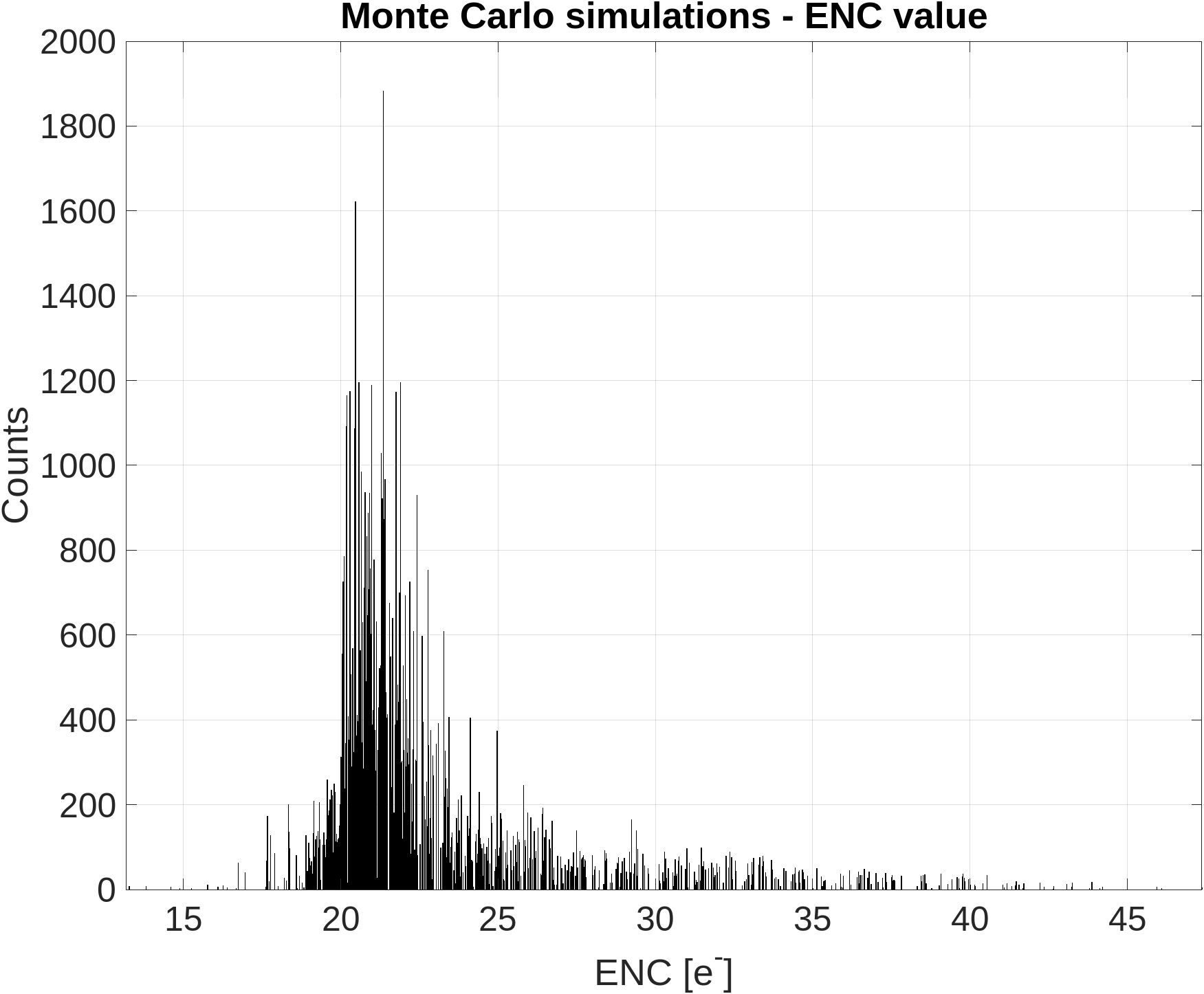
from the MC simulations (for 1000 runs), shown in Fig. 6,
reach 47 electrons rms for the worst case, which is not
very far from the specification. The summary of the MC
simulation is shown in Table 2.
The design underwent corner simulations to evaluate its
robustness under process, voltage, temperature (PVT) variations.
The worst ENC value that can be expected for fastfast
(ff) variation, minimal resistance and capacitance, maximum
temperature of 85 ◦C, is equal to 63 electrons rms.
This result suggests that, for operation at very high temperatures,
a proper cooling system may be mandatory. The
lowest achievable ENC is 16 electrons (slow-slow corner,
maximum resistance and capacitance, temperature -10 ◦C).
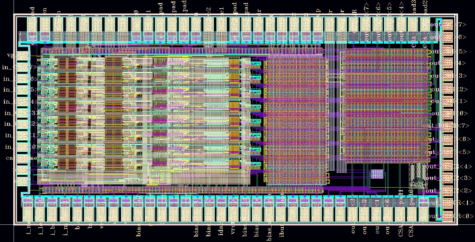
Design implementation
The design was implemented in a 180 nm complementary
metal-oxide-semiconductor (CMOS) process on a die of
1.5 µm × 3.2 µm area. Although the 180 nm CMOS technology
node is no longer considered cutting-edge in terms
of digital density, it offers several compelling advantages
for mixed-signal and radiation-tolerant applications. Its relatively
large feature size ensures better analogue performance,
higher supply voltage headroom, and greater resilience
to total ionizing dose (TID) effects, which are critical
for robust operation in harsh environments such as space,
high-energy physics experiments, or medical systems involving
high-intensity radiation sources. Apart from charge
processing channels, it also contains biasing circuits and
DACs, and a small area is occupied by another digital design
from a separate project – see Fig. 7. Post-layout simulations
demonstrated that the layout of the CSA reset circuitry is
critical to its proper operation and should be carefully optimised
to minimise coupling between the AFD control lines
and the CSAinput/output signal lines. To eliminate the CSA
baseline jumps, significant modifications were made to the
control line layout. After compensation, the baseline jumps
do not exceed 0.3 mV, which corresponds to approximately
5% of the CSA output amplitude for the default input charge
value (2200 electrons).
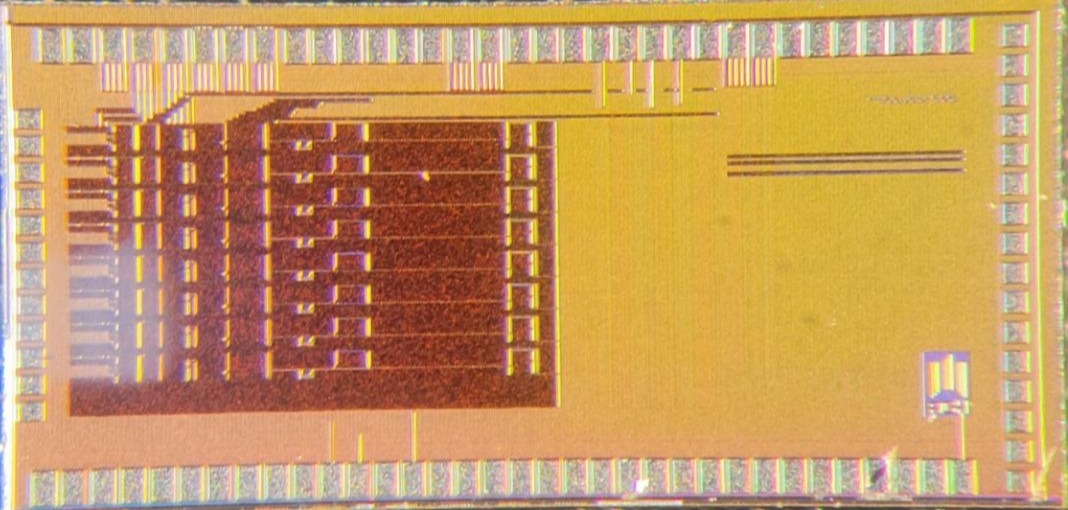
The design was submitted for fabrication in Q3 2024 and
is now ready for measurements – the ASIC photo is presented
in Fig. 8. Currently, the test setup is being designed,
including the test printed circuit board (PCB) dedicated
to wire-bonding of the ASIC. The PCB will be equipped
with all necessary biasing circuits and connectors. Signal
integrity tests will be performed using a mixed-signal oscilloscope
and a programmable pulse generator. In addition
to basic functional tests, noise measurements under varying
temperature and biasing conditions will be conducted to
confirm the simulation results. The presented IC comprises
an internal calibration circuit that allows for test charge injection
and basic characterisation of the read-out channels.
The tests with a semiconductor detector are also planned.
This work presents the design and characterisation of a lownoise,
high-resolutionCMOSread-out ASIC tailored for 1D
silicon strip X-ray detectors. The LNSTRIP prototype successfully
meets the stringent requirements of modern X-ray spectroscopy, offering an ENC below 50 electrons rms, low
power consumption under 10 mW per channel, and support
for high input rates through integrated fast reset and BLR
circuits. Simulation results, including MC and PVT corner
analyses, demonstrate robust performance and minimal
parameter variability in process variations. The fabricated
ASIC, implemented in the 180 nm CMOS technology, is
currently undergoing test preparations with further evaluation
planned using real detector systems. The developed
solution offers a compact and efficient front-end read-out
architecture, paving the way for its integration into highperformance
spectroscopic and imaging systems. Future
development of the presented architecture will focus on extending
the number of read-out channels and integrating
on-chip analogue-to-digital conversion. Additionally, efforts
will be directed toward implementing real-time digital
signal processing for hit detection and energy discrimination,
which would enable standalone operation without requiring
external back-end electronics. Testing in irradiation
and temperature-variable environments is also planned to
assess the long-term robustness of the ASIC.
Acknowledgements
The authors acknowledge funding of this project from
the National Science Centre (Research Project no. 137
2020/37/N/ST7/01546).
References
Geronimo, G., O’Connor, P., Radeka, V. & Yu, B. Front-end electronics for imaging detectors. Nucl. Instrum. Methods Phys. Res. A: Accel. Spectrom. Detect. Assoc.Equip. 471, 192–199 (2001).https://doi.org/10.1016/S0168-9002(01)00963-9.
Ballabriga, R. et al. Photon counting detectors for X-ray imaging with emphasis on CT. IEEE Trans. Radiat. Plasma Med. Sci. 5, 422–440 (2021).https://doi.org/10.1109/TRPMS.2020.3002949.
Wiacek, P. et al. Position sensitive and energy dispersive X-ray detector based on silicon strip detector technology. J. Instrum. 10, P04002 (2015). https://doi.org/10.1088/1748-0221/10/04/P04002.
Gerndt, E. & et al. Application of Si-strip technology to X-ray diffraction instrumentation. Nucl. Instrum. Methods Phys. Res. A: Accel. Spectrom. Detect. Assoc. Equip. 624, 350–359 (2010). https://doi.org/10.1016/j.nima.2010.05.032.
Zubrzycka, W. & Kasiński, K. Noise considerations for the STS/MUCH readout ASIC. In Toia, A. & Selyuzhenkov, I. (eds.) CBM Progress Report 2017, 32 (GSI Helmholtzzentrum für Schwerionenforschung, 2018). https://doi.org/10.15120/GSI-2018-00485.
Rossi, L., Fischer, P., Rohe, T. & Wermes, N. Pixel Detectors: From Fundamentals to Applications (Springer Berlin Heidelberg, 2006). https://doi.org/10.1007/3-540-28333-1.
O’Connor, P. & Geronimo, G. D. Prospects for charge sensitive amplifiers in scaled CMOS. Nucl. Instrum. Methods Phys. Res. A: Accel. Spectrom. Detect. Assoc. Equip. 480, 713–725 (2002). https://doi.org/10.1016/S0168-9002(01)01212-8.
Dabrowski, W., Bialas, W., Grybos, P., Idzik, M. & Kudlaty J. A readout system for position sensitive measurements of X-ray using silicon strip detectors. Nucl. Instrum. Methods Phys. Res. A: Accel. Spectrom. Detect. Assoc. Equip. 442, 346–354 (2000). https://doi.org/10.1016/S0168-9002(99)01248-6.
Grybos, P. Pole-zero cancellation circuit for charge sensitive amplifier with pile-up pulses tracking system. In IEEE Nuclear Science Symposium Conference Record (2006), 226–230 (IEEE, 2006). https://doi.org/10.1109/NSSMIC.2006.356145.
Zubrzycka, W. & Kasinski, K. All-programmable low noise readout asic for silicon strip sensors in tracking detectors. Nucl. Instrum. Methods Phys. Res. A: Accel. Spectrom. Detect. Assoc. Equip. 988, 164892 (2021). https://doi.org/10.1016/j.nima.2020.164892.
Zubrzycka, W. & Grybos, P. Optimization of low-noise read-out electronics for high energy resolution X-ray strip detectors. J. Instrum. 18, C01033 (2023). https://doi.org/10.1088/1748-0221/18/01/C01033.
Kleczek, R. et al. Single photon counting readout IC with 44 𝑒− rms ENC and 5.5 𝑒− rms offset spread with charge sensitive amplifier active feedback discharge. IEEE Trans. Circuits Syst. I: Regul. Pap. 70, 1882–1892 (2023). https://doi.org/10.1109/TCSI.2023.3241738.
Geronimo, G. D., O’Connor, P. & Grosholz, J. A CMOS baseline holder (BLH) for readout ASICs. IEEE Trans. Nucl. Sci. 47, 818–822 (2000). https://doi.org/10.1109/23.856523.
Dąbrowski, W., Fink, J., Fiutowski, T., Krane, H. G. & Wiącek, P. One dimensional detector for X-ray diffraction with superior energy resolution based on silicon strip detector technology. J. Instrum. 7, P03002 (2012). https://doi.org/10.1088/1748-0221/7/03/P03002.