In this study, we present the design and optimisation of a 2 × 4 quadrature phase and power splitter based on cascaded restricted interference-multimode interference (RI-MMI) couplers integrated with thermo-optic phase shifters on a silicon photonic platform. The device operates in the RI regime to achieve a compact, efficient configuration. The proposed circuit consists of two cascaded 2 × 2 RI-MMI couplers with integrated Ti-based heaters enabling precise thermo-optic phase control and switching capability. Numerical simulations using the 3D beam propagation method (BPM) show that the splitter performs effectively across a broad wavelength range of 1.5–1.6 μm, with an excess loss of approximately 0.2 dB at the central wavelength. The four output ports exhibit well-balanced power distribution, with a maximum deviation of about 15 dB, and maintain stable 90° phase differences among the outputs. The device also demonstrates robust thermal stability and tolerance to fabrication errors up to ± 1 nm, ensuring consistent optical performance. These findings highlight the strong potential of the proposed device for advanced optical signal processing applications such as quadrature phase-shift keying (QPSK) modulators, multicarrier phase-coded orthogonal frequency-division multiplexing (OFDM) systems, optical phasors, and multiphase local oscillators, providing a robust, high-precision platform that operates reliably across multiple wavelength bands.
Introduction
The rapid advancement of optical communication and signal processing technologies has driven demand for highly integrated, energy-efficient photonic systems. As data transmission rates continue to increase, the need for compact, stable, and broadband optical components has become more critical than ever. In this context, photonic integration offers a promising approach to overcoming the limitations of discrete optical elements by integrating multiple functionalities onto a single chip, thereby enhancing system performance, stability, and scalability.
Photonic integrated circuits (PICs) are critical to modern signal processing systems due to their ultra-high bandwidth, low-insertion loss, compact form factor, and cost-efficiency, with silicon-on-insulator (SOI)-based PICs being particularly attractive for their CMOS compatibility, low loss, and scalability for large-scale, cost-effective integration [1]. Among their core components, optical power splitters play a fundamental role by efficiently distributing optical signals from input sources to multiple outputs [2, 3]. Beyond power splitting, these devices can also introduce precise phase shifts between output ports, which are critical for advanced applications such as interferometric phasors [4], non-coherent vector detectors, and orthogonal frequency-division multiplexing (OFDM) systems [5]. High-performance splitters ensure not only balanced power distribution but also controlled phase relationships, directly impacting signal quality, loss, scalability, and system stability. Therefore, designing efficient power splitters is vital to advancing optical systems and data centre technologies.
Recent research efforts have focused on optimising power and phase splitters to achieve low-insertion loss and highly uniform power distribution, which are critical for reliable and efficient photonic systems. Multimode interference (MMI) devices have seen notable progress through various design strategies. For example, silicon nitride (Si3N4) MMI splitters have achieved insertion losses as low as 0.13 dB [6], offering stable power distribution ideal for data-centre applications. However, despite reduced back reflections, Si3N4 poses integration challenges with silicon-based platforms and is often limited to the O-band. In addition, inverse design approaches have further improved silicon splitters, achieving insertion losses below 0.76 dB and power uniformity within 0.84 dB [7], though fabrication imperfections such as etching misalignments and e-beam scattering remain limiting factors. Meanwhile, Y-branch splitters with rectangular waveguides have demonstrated minimal power imbalance (0.14 dB) across the C-band [8], but their fixed phase relationship renders them unsuitable for phase-sensitive applications.
Most prior studies have focused solely on optimising power distribution, overlooking phase control, thus limiting their use in phase-sensitive applications. This paper proposes a compact MMI-based power splitter using silicon waveguides with RI, featuring four output ports with a 90° phase shift between adjacent outputs. This design enables key applications such as orthogonal subcarrier generation, quadrature phase-shift keying (QPSK) modulators, and advanced Fourier-optic processing. In orthogonal subcarrier generation, the 90° phase spacing ensures orthogonality, which is crucial for phase-coded OFDM systems, enhancing spectral efficiency and reducing interference. In QPSK-loaded modulators, the phase-controlled outputs align naturally with modulation requirements, improving accuracy and simplifying system design. The proposed device is analysed using the mode propagation algorithm (MPA) and optimised via simulation, with performance validated through 3D beam propagation method (3D-BPM) simulations.
The remainder of this paper is organised as follows: section 2, optimised design and characteristic simulation, outlines the device structural configuration. Section 3, device performance characterisation, presents a detailed analysis of the device operation and performance, including comparisons with existing approaches. Finally, section 4, conclusions, summarises the key findings and contributions of this work.
Optimised design and characteristic simulation
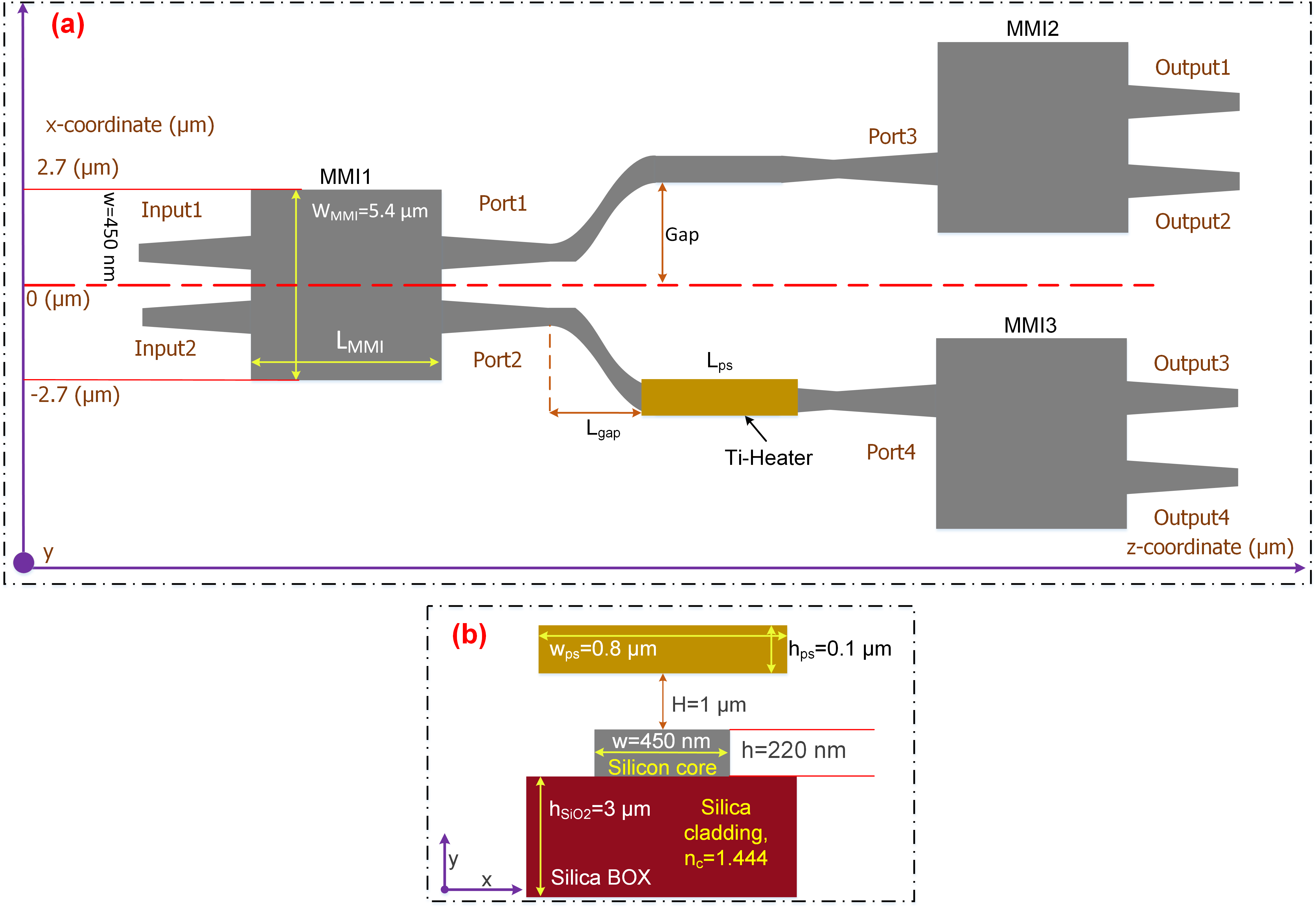
The conceptual diagram of the proposed device architecture, which employs a 2 × 2 RI-MMI coupler optimised for operation under transverse electric (TE) polarisation, is provided in Fig. 1(a) and 1(b). The design functions as a four-port power splitter, with the optical power equally distributed among all output ports and each output signal exhibiting a 90-degree phase shift relative to the others. This phase-controlled configuration is particularly suitable for coherent optical communication systems, such as those using QPSK modulation. The detailed design parameters are shown in both Fig. 1 and Table 1.
Fig. 1.The design structure of the proposed device based on a 2 × 2 MMI in the RI mechanism using
SOI waveguide platform: (a) schematic diagram and (b) cross-sectional view.
The side view that illustrates the structural geometry of the proposed device is shown in Fig. 1(a). Fig. 1(b) presents the cross-sectional view of the device at the light input region, corresponding to the single-mode access waveguide (Input1). The entire structure is implemented on a SOI platform, which consists of a 220 nm-thick silicon (Si) guiding layer and a 3 μm-thick buried oxide (BOX) layer made of silica (SiO2). This configuration is fabricated using a standard SOI wafer through CMOS-compatible semiconductor manufacturing processes.
The proposed design consists of two inputs (Input1 and Input2) and four outputs (Output1, Output2, Output3, and Output4), structured from a sophisticated combination of three RI-MMIs with the same width and length, two S-bend waveguides, and a titanium-based heater acting as a thermo-optic phase shifter (PS) for switching operation, as shown in Fig. 1(a). The tapered couplers were designed as isosceles trapezoids, characterised by a narrower bottom base width of 450 nm, a broader top base width of 900 nm, and a length of 30 μm. They have been initially selected. In this configuration, the conventional rectangular access waveguides for coupling to the multimode waveguide were replaced with tapered waveguides to provide input ports and output ports. When switching from single-mode to multi-mode waveguides, tapered waveguides were selected because they can improve light confinement, reduce the need for precise coupling lengths, and alleviate wavelength-sensitivity issues [9]. The axis of symmetry is defined as the centre line of the first MMI coupler in the propagation direction. To achieve high efficiency in the single-mode waveguide regime, the inputs and outputs with thinner bottom bases were connected to an access waveguide with a 450 nm thickness.
For every MMI coupler, the width of the RI-MMI coupler was initially chosen as WMMI = 5.4 μm. According to the theory, input and output ports of the RI-MMI are placed at the approximate positions of y = ± WMMI / 6 [10], two fold-images are reproduced at a length of LMMI = (2p + 1) Lπ / 2, with p = 0, 1, 2…, which is a non-negative integer and where Lπ is the half-beat length of the MMI coupler, which is defined by the following formula [10]:
where β0, β1 are corresponding to the propagation constants of the fundamental and first-order modes, respectively; λ0 = 1550 nm is the operation wavelength in the waveguides, and We is the effective width of the MMI coupler, which is calculated by the following formula under the TE polarisation state:
\(
W_c \simeq W_{M A M}+\left(\frac{\lambda_0}{\pi}\right)\left(n_r^2-n_c^2\right)^{-1 / 2}
\) (2)
Hence, the paired interference regime also exhibits two differently mirrored images at the shortest length of LMMI = Lπ/2. For a 2 × 2 RI-MMI, the effective index, neff, was approximately 2.59 using the BPM mode solver. Consequently, the calculated beat and self-imaging lengths were 70.8 μm and 35.4 μm, respectively. Moreover, our previous study has demonstrated that at a propagation length of 35.4 μm, the optical powers at the two output ports of the MMI are equal, confirming the 3 dB power-splitting condition [11]. Therefore, we choose an RI-MMI length of 35.4 μm for the proposed device.
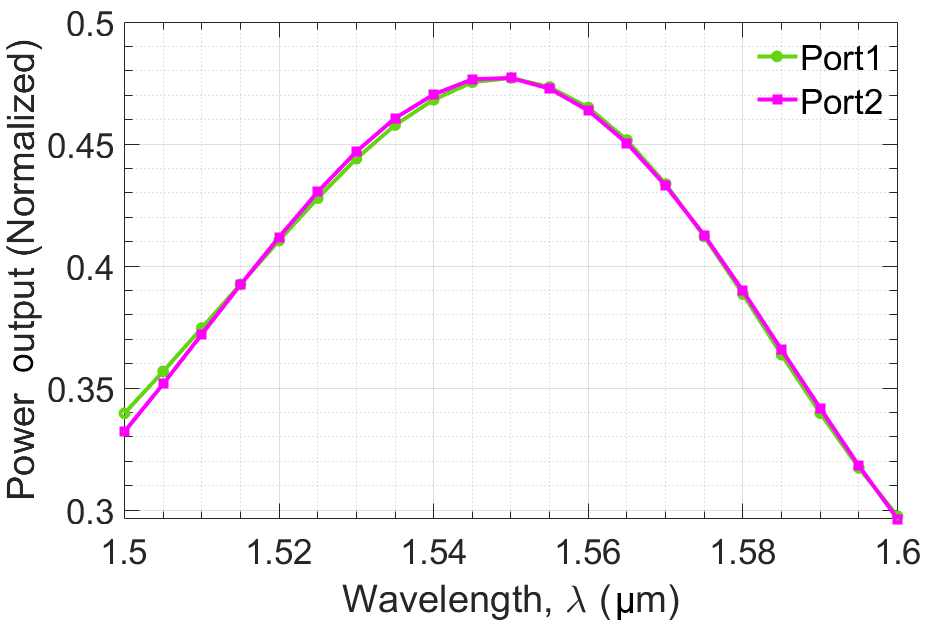
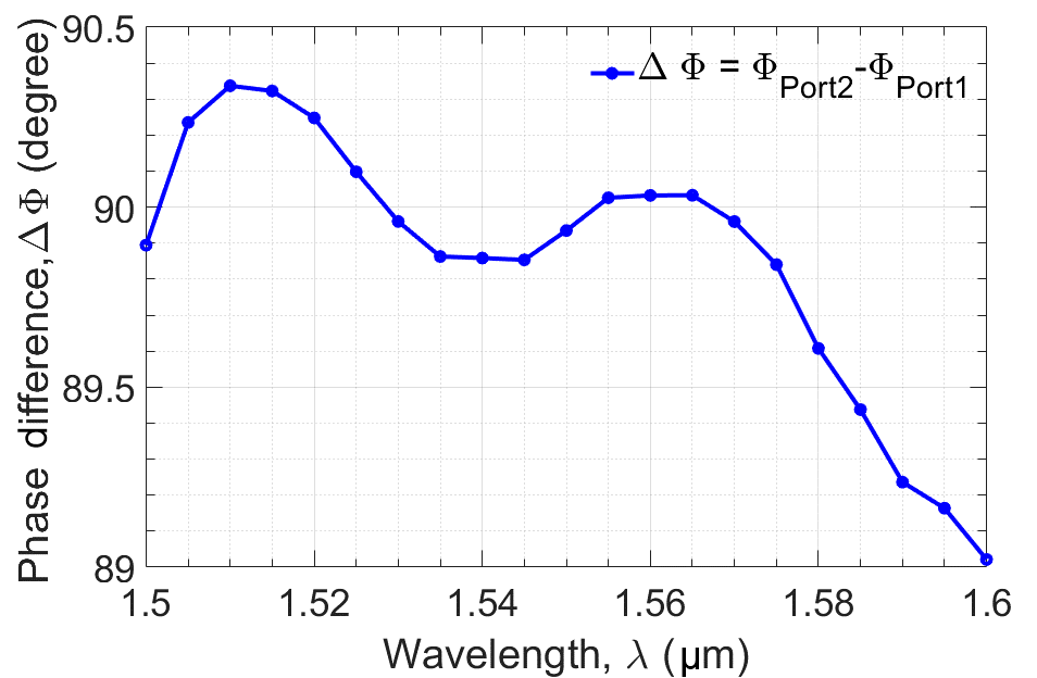
By applying the MMI theory [10], it is well known that in a 2 × 2 MMI coupler operating in the RI regime, each even mode leads its corresponding odd mode by a phase difference of π/2. This phase difference is determined by subtracting the phase angle of the mirrored output port (Port2) from that of the straightforward output port (Port1) at z = Lπ / 2 (referred to as the 3-dB length). As confirmed by simulation results in Fig. 2, when the MMI length reaches 35.4 μm [Fig. 2(a)], the device achieves equal power splitting across the operating wavelengths with a 90-degree phase difference between the two output ports [Fig. 2(b)].
Fig. 2. Optical performance wavelength-dependency of the
designed 3-dB power splitter based on the RI-MMI
coupler at LMMI = 35.4 μm for two output ports: (a) power
output (normalised) and (b) phase difference.
To interconnect the RI-MMI couplers and effectively split the optical paths, S-shaped bend waveguides are employed. These waveguides are designed with a length of 50 μm and a separation of 1.2 μm, enabling compact and efficient signal routing while minimising crosstalk and optical losses between adjacent paths.
In addition, a titanium (Ti) heater is placed along the second S-shaped waveguide (the lower branch). The heater has dimensions of 300 μm in length, 0.8 μm in width, and 0.1 μm in height, and is positioned 1 μm away from the silicon (Si) waveguide. This component functions as a PS and operates based on the thermo-optic effect. When the heater is heated (e.g., by an electric current), the resulting temperature change induces a local change in the refractive index, thereby causing a phase shift in the transmitted signal. This phenomenon is known as thermo-optic phase shifting (TOPS). In this design, our goal is to adjust the heater temperature to achieve a phase shift of precisely 90 degrees between the front and rear heaters. Consequently, a phase shift is introduced in the heated arm, altering the relative phase difference between the two arms of the interferometer to 180 degrees. This phase shift, arising from the thermo-optic effect, is quantitatively related to the refractive index change as expressed in the following equation [12]:
\(
\Delta \Phi=k \Delta n L_h
\) (3)
where Lh is the heater length in the propagation direction and k = 2π /λ is the wavelength number, n is the index change determined in relation with the thermal coefficient, dn /dT, and can be calculated as:
\(
\Delta n=\frac{d n}{d T} \Delta T
\) (4)
Here, the thermal coefficient for silicon is dn /dT = 1.84 × 10⁻⁴ K−1 at room temperature.
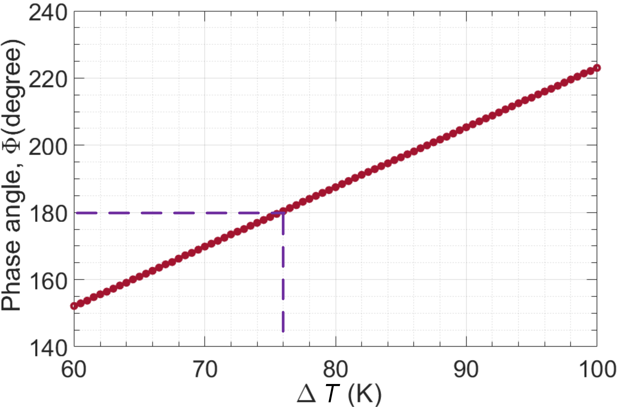
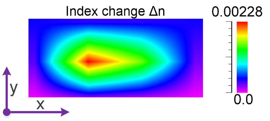
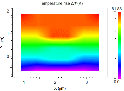
the TOPS mechanism. As shown in Fig. 3(a), the temperature-induced refractive index change occurs within the silicon layer beneath the heater. Fig. 3(b) presents the corresponding phase shift as a linear function of temperature increase (ΔT), derived from simulations using the commercial multi-physics tool RSoft. To achieve a phase shift of π radians, a temperature rise of approxi-mately 76 K is required, which aligns well with the theoretical relationship described in (3).
Fig. 3. The operation of the Ti-heater (TOPS): (a) phase angle as
a function of the temperature difference; (b) the index
change profile on the silicon layer of the Ti-heater
(TOPS) at ΔT = 76 K; (c) Ti-heater heat distribution
chart.
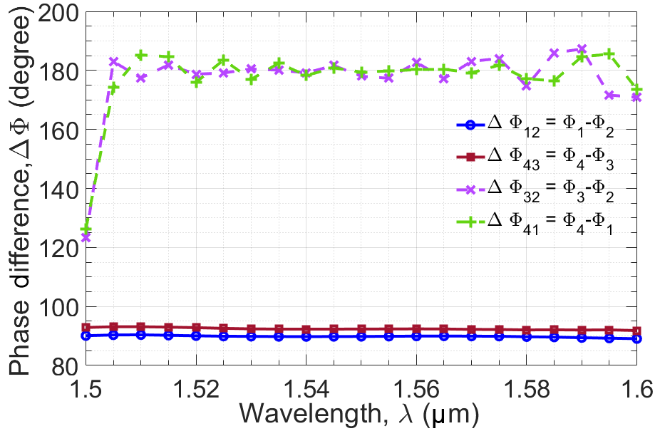
According to the proposed design, when light enters Input1 of the first MMI coupler, its phase is preserved at Port1 and Port2 is 90 degrees behind it. The signal from Port1 then propagates through an S-bend waveguide to Port3 without altering the phase relationship. Meanwhile, the signal from Port2 travels through another S-bend waveguide and passes through the TOPS, introducing an additional 90-degree phase shift. As a result, the phase at Port4 leads Port2 by 90 degrees and differs from Port3 by 180 degrees. In the second MMI, the signal at Port3 remains in phase with that at Port2 and is 90 degrees out of phase with Port1. Similarly, in the third MMI, the light at Port4 is in phase with Output3 and has a 90-degree phase shift relative to Output4. Consequently, Output3 differs from Output2 by 180 degrees, and Output4 is 180 degrees out of phase with Output1. To ensure optimal performance in advanced photonic applications, the power splitter must maintain consistent phase differences between output ports: ΔΦ₁₂ = Φ₁ − Φ₂, ΔΦ₄₃ = Φ₄ − Φ₃, ΔΦ₃₂ = Φ₃ − Φ₂, and ΔΦ₄₁ = Φ₄ − Φ₁. Stability in these phase differences is critical for minimising signal distortion and maintaining coherence in phase-sensitive systems.
Device performance characterisation
To evaluate the device performance, we also calculated the excess loss (EL) at each output port using the formulation in (5) [13]. For advanced photonic circuit applications such as interferometric phasors, non-coherent vector detectors, and phase modulation systems, our design must ensure that the phase differences between output ports (ΔΦ₁₂ = Φ₁ − Φ₂, ΔΦ₄₃ = Φ₄ − Φ₃, ΔΦ₃₂ = Φ₃ − Φ₂, ΔΦ₄₁ = Φ₄ − Φ₁) remain stable, with minimal variation, to guarantee reliable and precise signal processing.
where ELi is the excess loss of the ith output port, Pout_i and Pincorrespond to the ith output and input power, respectively.
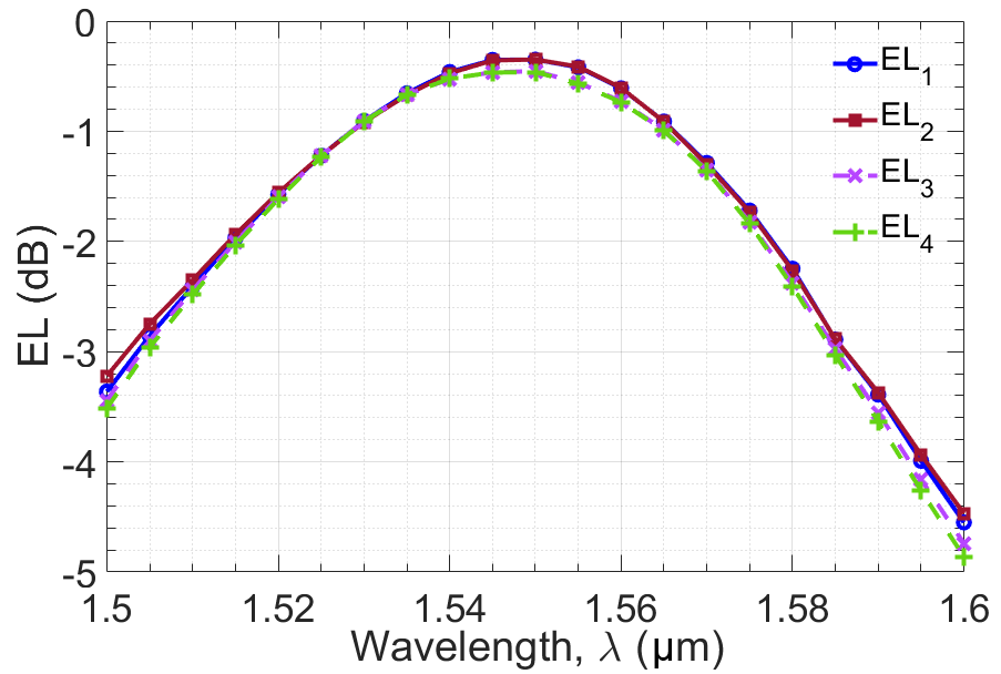
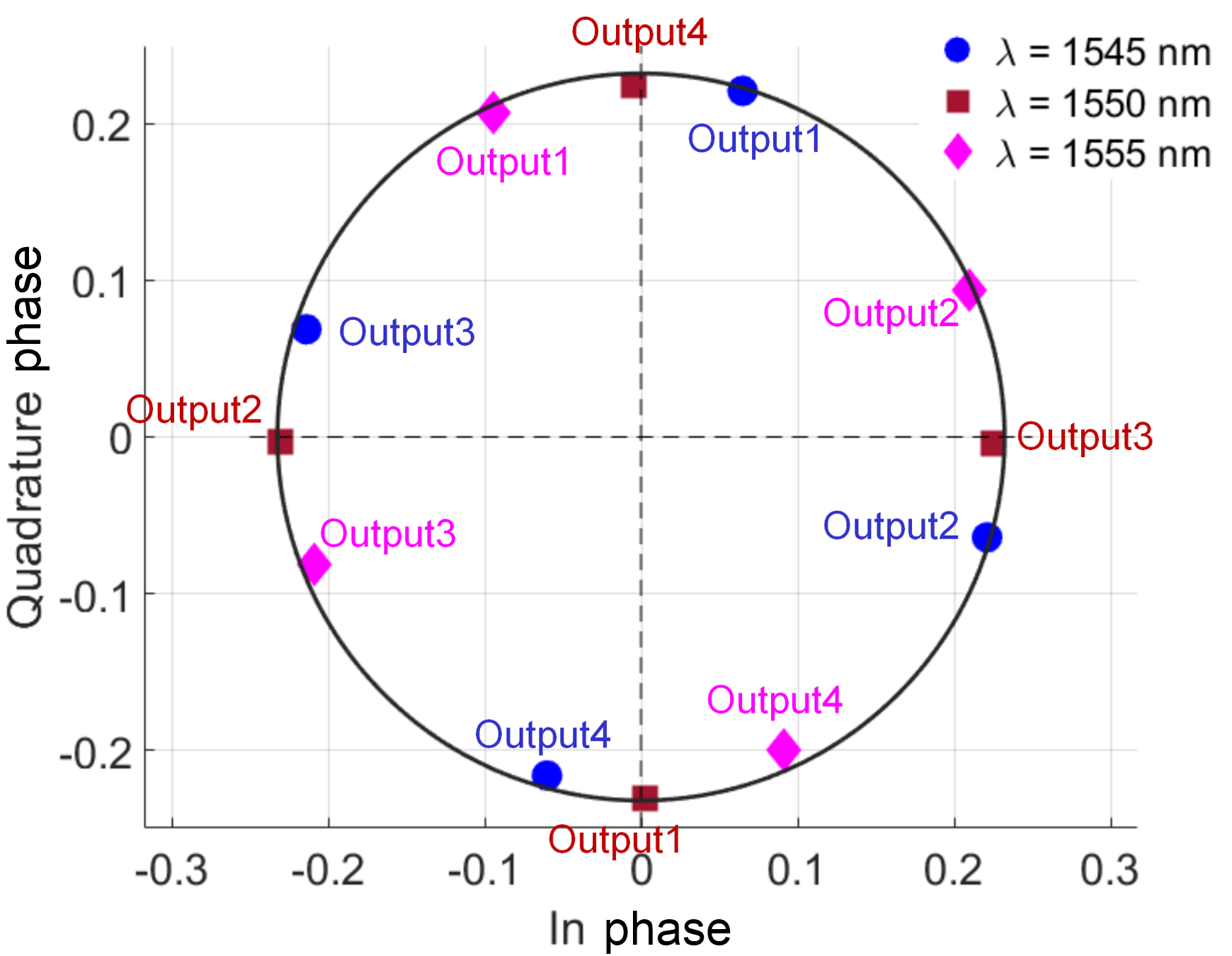
As illustrated in Fig. 4(a), the ELs across the four output ports remain nearly identical and follow smooth trends over a broad wavelength range from 1500 to 1600 nm, with a minimum loss of approximately 0.2 dB at 1550 nm. Fig. 4(b) presents the phase differences as a function of wavelength, showing stable quadrature relationships within the 1545–1555 nm range. Combining both amplitude and phase, Fig. 5 displays the output signal constellations. The output powers are evenly distributed and the phase relationships are nearly orthogonal across all three wavelengths. At the central wavelength, the constellation points align precisely at 0°, 90°, 180°, and 270°, while at the other two wavelengths, minor phase deviations are observed, with the relative 90° phase shifts well preserved. This demonstrates that the proposed device is highly suitable for applications such as orthogonal subcarrier generation, QPSK modulation, and advanced optical signal processing, where balanced power and strict phase control are essential for high performance and reliable operation.
Fig. 4. Optical performance wavelength-dependency of the
designed device in 100-nm spectra for four output ports:
(a) excess loss (EL) and (b) phase difference.
Fig. 5.Constellation diagram measured at 4 output ports of the
device at 1545 nm, 1550 nm, and 1555 nm wavelength.
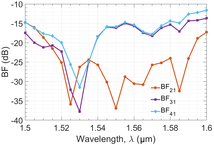
To evaluate the uniformity of power distribution, we applied standard equations to calculate the balance factor (BF), which helps identify devices achieving optimal 1:1:1:1 power splitting. The BF serves as a key metric for assessing performance consistency across output ports in devices such as splitters and couplers. It is defined as follows:
where Pout_i corresponds to the output power of Port2, Port3, and Port4, respectively. This formula shows the difference or balance of Port2, Port3, and Port4 compared to Port1. The simulation results of the ports BF based on the wavelength response from 1500 nm to 1600 nm are displayed in Fig. 6. Because BF is modest on the decibel scale, varying only from the maximum value of −12 dB to the lowest value of −38 dB, the simulation results demonstrate that the balance of the four ports is quite high owing to the device RI characteristics. Because BF = −15 dB, the balancing level is quite high at the centre wavelength of 1550 nm.
Fig. 6.Wavelength response balance factor of the proposed
power splitter ranging from 1500 nm to 1600 nm.
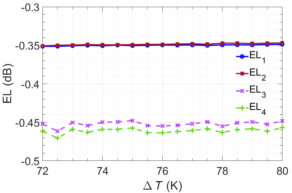
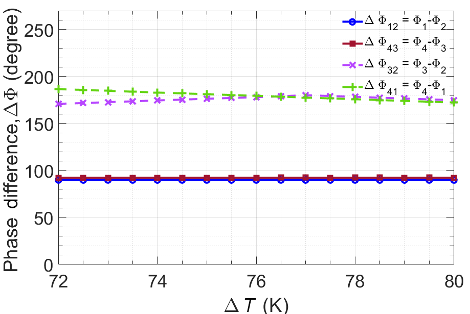
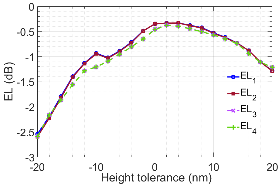
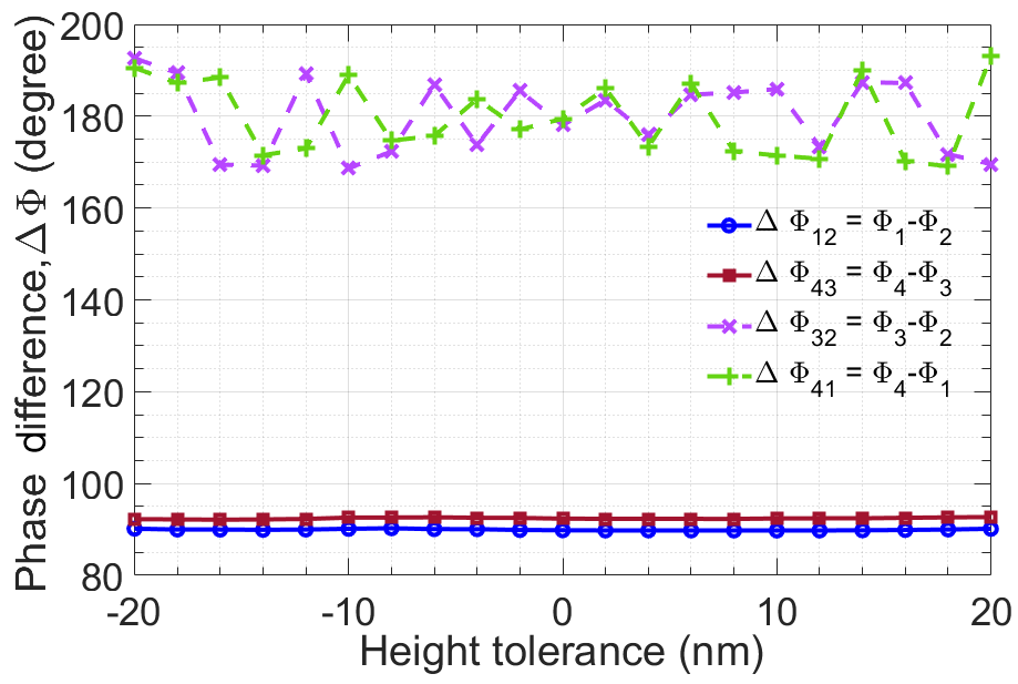
To optimise the thermal control efficiency of the heater, we investigated the impact of temperature variations on the heater, as illustrated in Fig. 7. Specifically, Fig. 7(a) shows EL as a function of the heater temperature, EL fluctuates at a low level from −0.45 dB to −0.35 dB, Fig. 7(b) shows the change of phase difference when the heater temperature changes. The results show that temperature changes have negligible effects on optical power. However, in terms of phase, the phase shift remains stable within a narrow temperature range around 76 K (specifically from 75 K to 77 K). Additionally, during device fabrication, the height variation of the silicon layer on the SOI platform is a critical parameter to consider. We examined the impact of this fabrication deviation, as shown in Fig. 8(a) and 8(b). The results indicate that the output power amplitude remains stable across the ports. However, to ensure phase accuracy, the permissible height deviation must be limited to ± 1 nm. Fortunately, with today’s advanced fabrication technologies, achieving this level of precision is entirely feasible.
Fig. 8. Optical performance height tolerance-dependency of the
designed device for four output ports: (a) EL and (b) phase
difference.
Conclusions
In conclusion, we proposed the design and optimisation of a cascaded RI-MMI-based 2 × 4 quadrature phase and power splitter integrated with thermo-optic PSs. The device operates effectively over the wavelength range of 1.5–1.6 μm, showing excellent performance within the C-band. At the central wavelength, the EL is approximately 0.2 dB, indicating low insertion loss, while the phase deviation among the output ports remains highly stable. Furthermore, the power balance across the four output ports is well maintained, with a maximum deviation of about 15 dB. The device also exhibits robust thermal stability, maintaining both low EL and stable phase characteristics under variations in heater temperature. In addition, even with fabrication tolerances of ± 1 nm, the splitter continues to perform reliably without significant degradation. Owing to these characteristics, the proposed device is highly promising for integration in coherent detection architec-tures and large-scale photonic integrated circuits.
Acknowledgement
Tran Thi Thanh Thuy was funded by the Master, Ph.D. Scholarship Programme of Vingroup Innovation Foundation (VINIF), code VINIF.2024.TS.084.
References
Izhaky, N. et al. Development of CMOS-compatible integrated silicon photonics devices. IEEE J. Sel. Top. Quantum Electron. 12, 1688–1697 (2006) https://doi.org/10.1109/JSTQE.2006.884089
Huang, J. Z., Scarmozzino, R. & Osgood, R. M. A new design approach to large input/output-number multimode interference couplers and its application to low-crosstalk WDM routers. IEEE Photonics Technol. Lett. 10, 1292–1294 (1998). https://doi.org/10.1109/68.705620
Turri, F., Biasi, S., Manzano, F. R. & Pavesi, L. A free-space interferometer for phase-delay measurements in integrated optical devices in degenerate pump-and-probe experiments. IEEE Trans. Instrum. Meas. 67, 2863–2871 (2018).
Liang, W. et al. Filterless vector light field photodetector based on photonic-electronic co-designed non-Hermitian silicon nanostructures. Opt. Express 33, 2395–2405 (2025). https://doi.org/10.1364/OE.550582
Frishman, A. & Malka, D. An optical 1 × 4 power splitter based on silicon–nitride MMI using strip waveguide structures. Nanomaterials 13, 2077 (2023). https://doi.org/10.3390/nano13142077
Kim, J. et al. Experimental demonstration of inverse-designed silicon integrated photonic power splitters. Nanophotonics 11, 20, 4581–4590 (2022). https://doi.org.10.1515/nanoph-2022-0443
Franata, N. & Purnamaningsih, R. W. Design of a 1 × 4 optical power divider based on Y-branch using III-nitride semiconductor.
Luo, Y., Yu, Y., Ye, M., Sun, C. & Zhang, X. Integrated dual-mode 3 dB power coupler based on tapered directional coupler. Sci. Rep. 6, 23516 (2016). https://doi.org/10.1038/srep23516
Soldano, L. B. & Pennings, E. C. M. Optical multi-mode interference devices based on self-imaging: principles and applications. J. Light. Technol. 13, 615–627 (1995). https://doi.org/10.1109/50.372474
Tran, T., Thanh, T., Trung, H. N., Nguyen, T. H. & Cao, D. T. 3D-BPM simulation design of a compact 3-dB optical power splitter using a 2 × 2 RI-MMI coupler on silicon waveguide. Opto-Electron. Rev. 33, e155674 (2025). https://doi.org/10.24425/opelre.2025.15567
Jacques, M. et al. Optimization of thermo-optic phase-shifter design and mitigation of thermal crosstalk on the SOI platform. Opt. Express 27, 10456–10471 (2019).
Qiyuan, Y. et al. Silicon MMI-based power splitter for multi-band operation at the 1.55 and 2 µm wave bands. Opt. Lett. 48, 1335–1338 (2023). https://doi.org/10.1364/OL.486428