Firmware development for the fibre-optic seismometer based on FOG
- Department of Microelectronics and Computer Science, Lodz University of Technology, ul. Wolczanska 221, 93-005 Lodz, Poland
- Institute of Applied Physics, Military University of Technology, ul. gen. Sylwestra Kaliskiego 2, 00-908 Warszawa, Poland
- Elproma Elektronika Sp. z o.o., ul. Duńska 2A, 05-152 Czosnów, Poland
Article Info
Received 15 Jan. 2024
Received in revised form 28 Feb. 2024
Accepted 13 Mar. 2024
Available on-line 15 Apr. 2024
Keywords: Fibre-optic rotational seismometer; Sagnac effect; simulation environment; field-programmable gate array; high-level synthesis.
Abstract
The main goal of the article is to present the concept of using a simulation environment when designing an advanced fibre-optic seismometer (FOS) using a field-programmable gate array (FPGA) computing system. The first part of the article presents the advanced requirements regarding the FOS principle of operation, as well as the measurement method using a closed-loop operation. The closed-loop control algorithm is developed using the high-level language C++ and then it is synthesised into an FPGA. The following part of the article describes the simulation environment developed to test the operation of the control algorithm. The environment includes a model of components of the measurement system, delays, and distortions in the signal processing path, and some of the measurement system surroundings. The article ends with a comparison of simulation data with measurements. The obtained results are consistent and prove correctness of the methodology adopted by the authors.
Introduction
Fibre-optic gyroscope (FOG) offers metrological parameters that are beyond the capacity of even the most advanced mechanical devices [1]. This device is the father of a group of others, including a fibre-optic seismometer (FOS) [2]. It is an advanced device dedicated to rotational seismology, which has become an emerging field for studying all aspects of rotational ground motions induced by explosions, earthquakes, and ambient vibrations [3]. The main difference between FOG and FOS is the final measured parameter, in the case of the former these are angular changes, whereas in the case of the latter it is the rotation rate [4]. It should be underlined that, generally, any seismograph is a more complicated device that contains general three components: seismometers – the sensors that detect seismic quantities, a recording system designed for data visualisation, and a network – the spatial distribution of a set of seismometers [5]. In this paper, the authors present their research on FOS. Although the basic operating principle of such FOS is quite straightforward and can be implemented in a relatively simple electronic system, many secondary effects adversely affect the performance – see section 2. Constructing a device that mitigates these problems calls upon much more involved electronics and complex control algorithms.
Usually, the first choice for the implementation of complex algorithms is a microprocessor system. Using a high-level programming language, such as C or C++, it is quite easy to express required computations. Moreover, a vast resource base gives the developer access to libraries and code snippets that handle commonly encountered problems. This approach also offers great capabilities for analysing the running program, known as debugging: the developer can easily trace program execution, investigate variables, output additional information, etc., which facilitates perfecting the code.
However, microprocessors are not without limitations. In particular, computation speed is often a limiting factor [6]. One must also remember that the seismograph is a portable device that might be battery-operated, thus, the microprocessor of choice will not be comparable in perfor-mance to the devices found in contemporary PCs. On the other hand, the required implementation must be fast to ensure high-end metrological parameters – see section 3. Eventually, the use of a microprocessor must be ruled out and the algorithm must be implemented differently.
Although application-specific integrated circuits (ASICs) may offer required speeds and at the same time low production costs due to the purpose-optimized design [7], their extremely high non-recurring engineering (NRE) costs make their use for prototyping or small-batch production prohibitive. For such scenarios, a field-programmable gate array (FPGA) is the approach of choice, allowing the designer to implement the algorithm as a programmable composition of logic gates and memory blocks [8]. Since the algorithm is expressed in this way, there is no overhead inherent to microprocessor systems, which pay for their flexibility with a time-consuming fetch–decode–execute cycle.
FPGA programming is usually performed using a hardware description language (HDL). Although it has significant advantages over schematic design, it is still not as well suited to algorithm implementation as the already mentioned programming languages for microprocessor systems. Moreover, it is challenging to analyse the execution of an algorithm expressed as an interconnection of logic gates.
Ultimately, one would like the best of both worlds: to design, implement, and develop an algorithm using a high-level programming language on a microprocessor system and to ensure high operating speed by running it on an FPGA circuit. Modern tools promise this; however, they are useless without a simulation environment that presents the algorithm with a digital twin of the device under control – in this case the FOS (a digital twin is a digital model of a real-world physical system that serves as an effectively indistinguishable digital counterpart of it).
This article presents an approach used by the authors to build such a twin and leverage the possibility of construct-ing FPGA-targeted algorithms using a PC-based simulation environment. The discussed results prove this approach to be effective. The authors believe the article may be useful for other developers of high-end optoelectronic devices, as it significantly speeds up the development process, thanks to the ease of testing new concepts and debugging the code.
The remainder of the article is organised as follows: section 2 outlines the concept of the FOS and section 3 presents project requirements for the target device. Section 4 introduces tools for FPGA programming in C++, while section 5 details the simulation environment used in the process. In section 6, some simulation results are presented and compared with experimental ones. The article offers conclusions in section 7.
Fibre-optic seismometer (FOS)
The measuring principle of FOS is based on Sagnac effect [9]. Sagnac device is a mirror-based ring inter-ferometer in which a collimated light source is split into two beams traveling in opposite directions along the same polygonal path. When these beams meet, an interference pattern may be observed. Rotating a device around the axis perpendicular to the path plane means that when the clockwise (cw) beam arrives at the meeting point, this point has already slightly moved in the rotation direction. Consequently, the path of the cw wave is longer than the counterclockwise (ccw) wave, and the fringe pattern is offset due to the phase difference Δ𝜙𝜙R [10].
The FOS based on optical fibre replaces the mirror-based setup. Optical fibre allows making very long paths in a compact device by winding the fibre on a carcass. It is possible to obtain a path length of several kilometres using a coil that is 60 cm in diameter [11]. This greatly increases the sensitivity of the device, as the difference in paths increases with the path length. The phase difference due to rotation is given by [12]
\( \Delta \phi_{\mathrm{R}}=\frac{2 \pi L D}{\lambda c} \Omega \) (1)
where 𝐿 is the fibre length, 𝐷 is the coil diameter, 𝜆 is the wavelength, 𝑐 is the speed of light, and 𝛺 is the rotation speed.
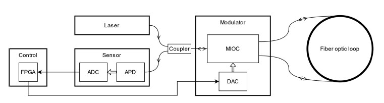
In order to obtain high sensitivity of the device, several concepts, both hardware and software, must be employed. As for the hardware, a full-reciprocal design, the so-called FOG minimum configuration eliminates many detrimental effects, such as parasitic interference fringes or phase drift [13, 14]. The main components of the FOS hardware are presented in Fig. 1. The source of light is a Laser connected to a fibre-optic loop via a Coupler and a multi-functional integrated optical chip (MIOC) located on the Modulator. The Modulator is an electronic hardware equipped with a digital-to-analogue converter (DAC) and its function is to control the phase of light wave through a digital interface. The sensor using an avalanche photodiode (APD) and an analogue-to-digital converter (ADC) allows a digital readout of the returning light power. The control module with the FPGA is the heart of the FOS control system. It executes the algorithm, collects output data, manages electronic components, and provides interface to the device.
The controlling software, or firmware, as it is embedded in the FPGA device, must implement several approaches, some of which are briefly outlined below:
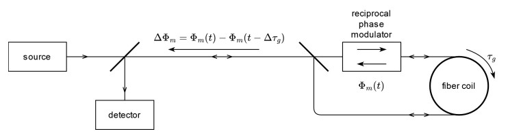
- because the optical power response of the fringe pattern is proportional to cos(Δ𝜙R), there is a need to provide a bias to move the operating point with a non-zero response slope. This is done using a square-wave modulation with a period of 2Δ𝜏g, where Δ𝜏g is the group transit time through the coil. It uses a reciprocal phase modulator placed at one end of the coil ( Fig. 2) and acts as a delay line [15]:
- due to the inaccuracy of the modulation wave period and limited response time of the hardware, spikes may appear in the power response – these have to be filtered out before computations;
- to provide good performance over the entire measurement range, closed-loop operation [16], which maintains an operating point close to the optimum regardless of the measured rotation speed, should be employed;
- closed-loop operation requires an additional phase-nulling signal which cancels Δ𝜙R. This signal is generated using a digital ramp with step 𝜙S= −Δ𝜙R. Since the ramp signal cannot rise infinitely, it must be periodically reset to a lower value, which is an additional source of measurement noise;
- modulation may use a four-state signal instead of a two-state one [17], additional states are useful for deter-mining the gain of the modulation chain, which directly influences the computed value of the rotations speed.
Project requirement
The designed device is intended to be universally applicable in rotational seismology, both for research in engineering applications [2] (monitoring vibrating move-ments of tall, irregularly shaped buildings, wind farms, chimneys, rock mass activity, etc.) and for seismological research [18]. Other solutions available on the market are focused on only one of these applications – either engineering research or seismological research. This means that the presented device must meet very difficult design assumptions, both in terms of measurement parameters (measuring range and frequency) and operational para-meters (mobility, autonomy, power supply independence, environmental stability). Extremely high sensitivity of several dozen nrad/s (three orders of magnitude below the Earth’s rotation speed of approximately 73 μrad/s), as well as dynamics: up to approximately 10 rad/s (nine orders of magnitude, i.e., dynamics of 180 dB) are required. Additionally, the measurement system should be characterised by a linear characteristic in the assumed band from 0.01 Hz to 100 Hz and a low noise level: angular random walk (ARW) – a described system sensitivity of order of 50 nrad/√𝑠, bias instability (BI) – a described system stability below 30 nrad/s determined from Allan characteristics [19, 20]. Such high measurement requirements result in the need to create an optical system with appropriate sensitivity and low loss, coupled with a specialised closed-loop digital signal processing system.
High-level synthesis
During the implementation of the algorithms, the authors have decided to use high-level synthesis (HLS) as a primary design tool. The main reasons behind this decision were:
- complexity of the data-processing algorithm, involving,
- many fixed-point operations (addition, multiplication, and division) on data of varying width,
- fast implementation with C++,
- fast verification of the implementation at the C++ level.
A typical workflow using HLS is presented in technical manuals [21] and involves the following steps:
- design entry (C++, C or SystemC),
- functional verification – test benches implemented in high-level languages,
- register-transfer level (RTL) generation,
- RTL simulations as the final verification step.
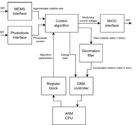
HLS was used to synthesise the FOS control algorithm. The control algorithm is implemented as a C++ function, with a stream of samples representing the APD current at the input and a stream of MIOC control voltages at the output. The input and output sampling rates are 1 MS/s. Therefore, the processing time of the control algorithm must be lower than 1 μs. The system was implemented using the Xilinx Zynq SoC platform [22]. The block diagram of the system firmware is presented in Fig. 3. The ADC and DAC were connected using SPI interfaces. The firmware components interacting with the external hardware and the integrated advanced RISC machines (ARM) CPU were written in a very high-speed integrated circuit hardware description language (VHDL) due to specific timing and interface requirements difficult to meet otherwise. The output decimation filter has been designed using a Xilinx filter generator.
Simulation environment
The developed simulation environment is the core of the discussed approach. It is outlined in Fig. 4 and consists of:
- rotation generator (RG),
- digital twins of the hardware components used in the
- FOS: modulator gain generator (MGG), maximum power generator (MPG), MIOC filter (MF), sensor (S)
- code for FPGA under development: control algorithm (CA), median filter (MF), output filter (OF),
- interconnections between the above elements,
- possibility for using collected data in input.
Since in real-life operations the control algorithm is executed for every sample acquired from the input ADC converter, the simulation loop is executed in the same manner. In each computational cycle, individual components retrieve data from the input streams, perform calculations, and generate data sent to the output streams. HLS streams, which are compatible with the synthesis requirements, were used for data interchange. The components of the simulation environment are discussed in the subsequent sections.

Rotation generator
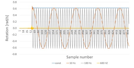
This component is responsible for generating angular velocity signal. The signal waveform may be:
- linearly increasing,
- rectangular,
- sinusoidal,
- constant,
and developer may easily change parameters of the waveform prior to running the simulation. The generated signal is directly fed to the sensor component.
Sensor
The component is responsible for modelling several analogue elements in the measurement path: MIOC modulator, fibre-optic loop, detection diode, and simulation environment ADC and DAC. Its task is to compute the power of light beam, as received by a detection diode, based on a generated analogue angular velocity signal and a digital signal from the control algorithm. The core of the component, expressed in C++ programming language, is presented in Listing 1.

The model also includes two basic sources of noise: the output of the sensor (photodiode) and the input of the MIOC modulator. Both sources produce white noise with an amplitude adjusted by a program parameter. Noise naturally hinders the operation of the feedback loop because it does not allow the error signal to be fully cancelled and causes constant instability of the system (Fig. 5). Code snippet responsible for introducing noise is presented in Listing 2.


FPGA code
This component contains functionality that, after synthesis, is to be placed in the FPGA circuit. Most of the code is subject to HLS, i.e., is written in C++; HLS tools ensure that identical operation is guaranteed during simulation and operation in the target FPGA device. The output filter block was designed differently and is thus discussed in a separate section. Of the remaining two component blocks, the control algorithm block is a more complicated one and contains the following functionalities (see section 2 for an explanation of these functionalities):
- generation of a four-state modulation signal (Fig. 6 and Fig. 7 – orange line);
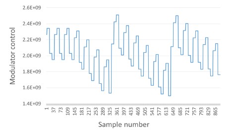
- controllers for the ramp step height 𝜙S and gain of the modulation chain. The operation of the ramp step controller is shown in Fig. 8;
- support for ramp reset at 2𝜋 intervals;
- computation of the final signals for the DACs that drive the MIOC modulator.

MIOC filter
The component is responsible for modelling distortions. at the input of the MIOC system. The MIOC system has a capacitive input which results in a significant rise time of the signal. This causes additional power spikes to appear on the sensor system (Fig. 9 and Fig. 10) and further complicates control. The capacitive character of the model was achieved thanks to the use of a filter with an infinite impulse response (see Listing 3).


The problem was the selection of filter parameters, which in the first version were significantly exaggerated and distortions were too strong. The measurements performed at the input of the MIOC system showed that the rise time is much smaller than initially assumed and is approximately 1 μs. Since the sampling frequency of the real system is 1 MHz, the phenomenon of a signal rise could not be properly modelled: duration of rise is equal to time between two adjacent samples. For this reason, it was decided to introduce oversampling for the analogue part of the system with a frequency of 10 MHz. At the interface between the digital and analogue parts, a "wrapper" was included, which allows for matching signals from both parts with different sampling rates.

Output filter
The final component of the measurement path is a finite impulse response (FIR) filter smoothing the final response of the device (the measured angular velocity). This component is located outside the closed-loop path and, thus, is not subject to time constraints. It was decided to use a cascade of decimation filters (more difficult to design and with a more shape characteristics than FIR filter) of a lower order, thus consuming smaller hardware resources and minimizing the power generated in the FPGA system than FIR filter. The decimation filter was automatically generated directly in a FPGA-implementable version, using dedicated Xilinx tools. At the same time, C++ counterpart working with HLS streams was generated using these tools, for inclusion in the simulation environment. Unfortunately, an analysis of the generated code showed significant flaws, preventing its proper use. Since the filter is not part of the feedback loop, HLS-based approach was abandoned and a simpler model, operating on buffers, was programmed independently for simulation. Ultimately, a six-stage decimation filter was used. The final effect obtained is shown in Fig. 11.
Simulated vs. experimental results
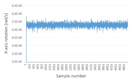
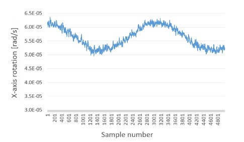
Experimental research on the measurement system was carried out in two different ways. The first method was possible due to the high sensitivity of the system and based on detecting small and stable rotation speed – the device was used to measure the rotation speed of the Earth (in the measurement laboratory in Lodz, Poland this rotation speed was 53 μrad/s). This result is consistent with the theoretical value of rotation speed calculated from the following formula obtained on a simple graphical interpretation shown in Fig. 12:
\( \omega=\omega_0 \sin \alpha \) (2)
where 𝜔0 is the Earth’s rotation speed of 73 μrad/s, 𝜔 is the rotation speed measured on Earth’s surface at a given latitude 𝛼.

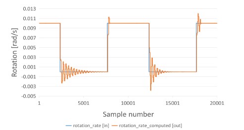
The subsequent plots (Fig. 13 and Fig. 14) present simulation results for two different settings of an internal parameter defining the number of modulation periods for which the input (optical) power is averaged – longer averaging intervals (Fig. 14) give smoother output at the expense of response time.

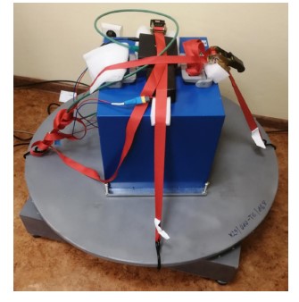
The comparison of the above simulations with experi-mental results (Fig. 15 and Fig. 16) obtained for the developed fibre-optic rotational seismometer FOS6-02 (an element of the FOSREM project – see acknowledgements) shows some differences in the system startup (in the simulation, the system is buffered during startup) and the presence of additional noise coming from the external environment of the system (mechanical shocks, network ripples, etc.). However, it should be underlined that sensitivity of FOS6-02 is very high (measured ARW in the range of 45 nrad/√𝑠,).While the first method checked capabilities of the system to measure very small rotational speeds, the second method covered the other end of the measurement range. It involved a manually controlled, electrically-powered rotating platform, operating in the range from −10 rad/s to 10 rad/s (Fig. 17). A MEMS gyroscope (LSM6DSO32 – 3D digital accelerometer and 3D digital gyroscope by STMicroelectronics) placed on the platform and an additional external electromagnetic gyroscope observing the marker on the rotating platform were used as reference. In the experiment, the FOS6-02 has been used.

The results of the above experiment are presented in Fig. 18. They are nearly identical which confirms the correctness of the simulation approach described insection 5. They also confirm the ability of the designedFOS6-02 fibre-optic rotational seismometer to measurevery high rotational speeds in the range of 10 rad/s withgood linearity (no worse than commercially availableelectronic gyroscope).

The usefulness of the simulation based on PC can beshown by comparing the time savings resulting from theuse of the PC instead of FPGA. Table 1 summarises stepsand related times required to introduce changes to thealgorithm code and run this code to observe impact of thechanges. To fully recognise the time savings, one mustremember that such a procedure is repeated thousands oftimes during the development of an algorithm ascomplicated as in the presently discussed case.
Table 1.
Steps and times required to introduce and evaluate changes in the algorithm code.
Step |
Typical time [s] |
|
|
FPGA |
PCa |
built project |
2400 |
20 |
program device |
60 |
N/A |
runb,c |
10 |
77 |
total |
2470 |
97 |
Conclusions
The plots presented in the previous section show a very good conformity between the simulation and experimental results. This is particularly visible for the large measure- ment signals where the curves look virtually identical. For small rotation speeds, the measured value and the overall behaviour of the system are the same, the only discrepancy is somewhat different character of the noise component: noise in the measurement data is more visible and variable in time, moreover, there are spikes placed at regular interval. This shows some limitations of the simulation environment that leaves room for the improvement.
The conformity between simulation and experiment proves that the PC-based simulation environment can be successfully used to develop algorithms for the FPGA-based device. One of the most important advantages is the time saving resulting from the use of the PC-based simulation, which paves the way for more effective research procedures.
Authors’ statement
The research concept and design, W.T., G.J., and L.R.J.; collection and/or assembly of data, R.K.; data analysis and interpretation, M.K.; writing the article, M.K., R.K., and W.T.; critical revision of the article, L.R.J.; final approval of article, B.S., W.T., P.A., and R.K.
Acknowledgements
This work has been made under financial support of the National Centre for Research and Development project POIR.01.01.01-00-1553/20-00 “FOSREM – from Sky across Ground up to Underground”.
References
-
Lefẻvre, H. C. The Fibre-Optic Gyroscope. 2nd Ed. (Artech House, 2014).
-
Jaroszewicz, L. R. Review of the usefulness of various rotational seismometers with laboratory results of fibre-optic ones tested for engineering applications. Sensors 16, 2161 (2016). htpps://doi.org/10.3390/s16122161
-
Lee, W. H. K., Celebi, M., Todorovska, M. & Igel, H. Introduction to the special issue on rotational seismology and engineering applications. Bull. Seismol. Soc. Am. 99, 945–957 (2009). https://doi.org/10.1785/01.20080344
-
Jaroszewicz, L. R, Dudek, M., Kurzych, A. T. & Teisseyre, K. P. A test performance of optical fibre sensors for real-time investigations of rotational seismic events: a case study in laboratory and field conditions. Opto-Electron. Rev. 29, 213–219 (2021). https://doi.org/10.24425/opelre.2021.140102
-
Havskov, J. & Alguacil, G. Instrumentation in Earthquake Seismology. 2nd Ed (Springer, 2016).
-
DiVincenzo D. Computers are becoming faster and faster, but their speed is still limited by the physical restrictions of an electron moving through matter. What technologies are emerging to break through this speed barrier? SCIAM (Accessed: Dec. 31st, 2023)https://www.scientificamerican.com/article/computers-are-becoming-fa/
-
Max Maxfield, C. M. Bebop to the Boolean Boogie. An Unconventional Guide to Electronics, 3rd Ed. 235–249, (Elsevier Inc., 2009). https://doi.org/10.1016/B978-1-85617-507-4.X0001-0
-
Lin, M. & El Gamal, A. A low-power field-programmable gate array routing. IEEE Trans. Very Large Scale Integr. (VLSI) Syst. 17, 1481–1494 (2009). https://doi.org/10.1109/TVLSI.2008.2005098
-
Sagnac, G. L’éther lumineux démontré par l’effet du vent relatif d’éther dans un interféromètre en rotation uniforme. C. R. Acad. Sci., 157, 708–710 (1913). (IN FRENCH).
-
Post, E. J. Sagnac Effect. Rev. Mod. Phys. 39, 475–494 (1967). https://doi.org/10.1103/RevModPhys.39.475
-
Jaroszewicz, L. R., Krajewski, Z. & Teisseyre, K. P. Usefulness of AFORS – Autonomous fibre-optic rotational seismograph for inves- tigation of rotational phenomena. J. Seismol. 16, 573–586 (2012). https://doi.org/10.1007/s10950-011-9258-3
-
Vali, V. & Shorthill, R. W. Fibre ring interferometer. Appl. Opt. 15, 1099–1100 (1976). https://doi.org/10.1364/AO.15.001099
-
Ulrich, R. Fibre-optic rotation sensing with low drift. Opt. Let. 5, 173–175 (1980). https://doi.org/10.1364/OL.5.000173
-
Arditty, H., Papuchon, M. & Puech, C. Ring Interferometer Device and Its Application to the Detection of Non-Reciprocal Effects. U.S. Patent # 4 480 915 (1984).
-
Martin, J. M. & Winkler, J. T. Fibre-optic laser gyro signal detection and processing technique. Proc SPIE. 139, 98–103 (1978). https://doi.org/10.1117/12.956249
-
Lefèvre, H. C., Vatoux, S., Papuchon, M. & Puech, C. Integrated optics: a practical solution for the fibre-optic gyroscope. Proc SPIE. 719, 101–112 (1986). https://doi.org/10.1117/12.937545
-
Lefèvre, H. C. & Martin, P. Optical-Fibre Measuring Device Gyrometer, Central Navigation And Satisfying Systems. U.S. Patent # 5 141 316 (1992).
-
Bernauer, F., Wassermann, J. & Igel, H. Rotational sensors—a comparison of different sensor types. J. Seismol. 16, 595–602 (2012). https://doi.org/10.1007/s10950-012-9286-7
-
IEEE Standard Specification Format Guide and Test Procedure for Single-Axis Interferometric Fibre Optic Gyros, IEEE-SA Standards Board 952 (1998).
-
Allan Variance: Noise Analysis for Gyroscopes. Freescale Semiconductor Inc. (2015). https://telesens.co/wp-content/uploads/%202017/05/AllanVariance5087-1.pdf
-
ug902 HLS User Guide. (Acessed: Nov. 21st, 2023). https://www.xilinx.com
-
KRIA 26. Xilinx (Acessed: Nov. 21st, 2023). https://www.xilinx.com/products/som/kria/k26c-commercial.html